Method for manufacturing through substrate via (tsv), tsv structure of through silicon via and control method of tsv capacitance

A manufacturing method and substrate technology, which are used in semiconductor/solid-state device manufacturing, circuits, electrical components, etc., to improve signal interference problems and avoid attenuation.

Inactive Publication Date: 2014-01-22
IND TECH RES INST
View PDF5 Cites 0 Cited by
  • Summary
  • Abstract
  • Description
  • Claims
  • Application Information

AI Technical Summary

Problems solved by technology

[0006] The invention provides a method for manufacturing a substrate through-hole structure, a substrate through-hole structure, and a method for controlling the capacitance of the substrate through-hole. The potential of the substrate surface and the bottom is almost the same through a groove containing a low-resistance material to precisely control the electric potential of the conductive via hole. The generated coupling capacitors and other components can improve the substrate noise and the signal interference between the conductive vias

Method used


Image

  • Method for manufacturing through substrate via (tsv), tsv structure of through silicon via and control method of tsv capacitance
  • Method for manufacturing through substrate via (tsv), tsv structure of through silicon via and control method of tsv capacitance
  • Method for manufacturing through substrate via (tsv), tsv structure of through silicon via and control method of tsv capacitance

Examples


no. 1 example

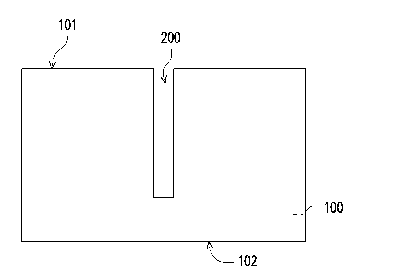
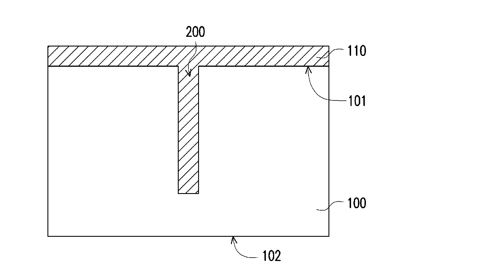
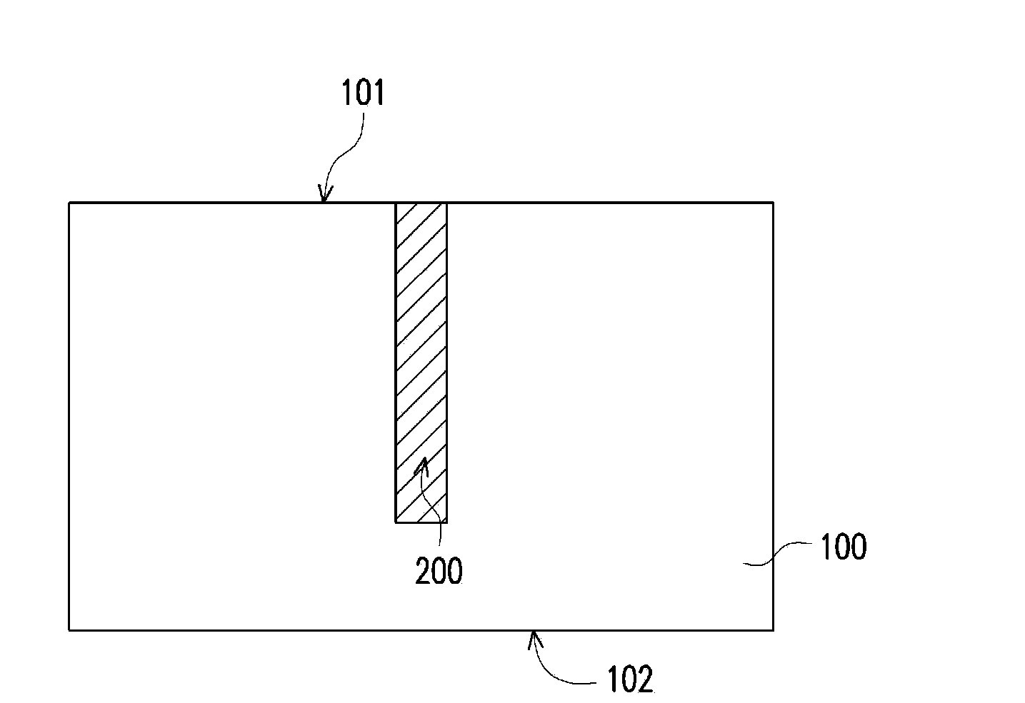
[0058] Figure 1 to Figure 12 is a schematic flow chart of the manufacturing method of the through-substrate structure according to the first embodiment of the present invention. First please refer to figure 1 , a substrate 100 is provided, and the substrate 100 has a first surface 101 and a second surface 102 . According to an embodiment of the present invention, the substrate 100 is, for example, a silicon substrate (such as a wafer) or other suitable semiconductor substrate materials. In general, the first surface 101 of the substrate 100 may be referred to as a back surface, and the second surface 102 of the substrate 100 may be referred to as a top surface. Furthermore, a trench 200 is formed on the first surface 101 of the substrate 100 . Here, the method of forming the trench 200 is, for example, using the photoresist layer on the first surface 101 as an etching mask, and the photoresist layer has an opening at the position of the trench 200 to etch the substrate 100...

no. 2 example

[0073] Figure 14 to Figure 20 is a schematic flowchart of a method for manufacturing a through-substrate structure according to a second embodiment of the present invention. The main difference between the second embodiment and the first embodiment lies in the sequence adjustment of each manufacturing step, so please refer to the above-mentioned first embodiment for details not mentioned here. First please refer to Figure 14 , a substrate 100 is provided, and the substrate 100 has a first surface 101 and a second surface 102 . Moreover, an insulating layer 120 is formed on the first surface 101 of the substrate 100 . In this embodiment, the insulating layer 120 is a three-layer insulating layer formed sequentially, such as a first silicon nitride layer 121 , a first silicon oxide layer 122 and a second silicon nitride layer 123 .

[0074] Please refer to Figure 15 , forming at least one opening on the first surface 101 of the substrate 100 . The embodiment of the prese...

no. 3 example

[0077] Figure 21 to Figure 26 is a schematic flowchart of a method for manufacturing a through-substrate structure according to a third embodiment of the present invention. The main difference between the third embodiment and the above-mentioned first and second embodiments lies in the sequence adjustment of each manufacturing step, so please refer to the above-mentioned first and second embodiments for details not mentioned here. First please refer to Figure 21 , a substrate 100 is provided, and the substrate 100 has a first surface 101 and a second surface 102 . Moreover, an insulating layer 120 is formed on the first surface 101 of the substrate 100 . Then, at least one opening and the trench 200 are simultaneously formed on the first surface 101 of the substrate 100 , and the embodiment of the present invention takes two openings 210 , 220 as an example.

[0078] Please refer to Figure 22 , sequentially form the oxide circuit layer 130 , the barrier layer 140 and th...


PUM

PropertyMeasurementUnit
diameteraaaaaaaaaa
diameteraaaaaaaaaa

Abstract

A method for manufacturing a through substrate via (TSV) structure, a TSV structure, and a control method of a TSV capacitance are provided. The method for manufacturing the TSV structure includes: providing a substrate having a first surface and a second surface; forming a trench in the first surface of the substrate; filling a low resistance material into the trench; forming an insulating layer on the first surface of the substrate; forming at least one opening in the first surface of the substrate, wherein the opening is located differently the trench; forming an oxide liner layer, a barrier layer and a conductive seed layer on a sidewall and a bottom of the opening and on the insulating layer of the first surface; and filling a conductive material into the opening. Thus, the through substrate via (TSV) structure can reduce a noise problem of the substrate.

Description

technical field [0001] The present invention relates to a chip stacking technology, and in particular to a manufacturing method of a TSV, a structure of the TSV and a method for controlling the capacitance of the TSV. Background technique [0002] With the continuous advancement of semiconductor technology, in order to improve the integration of semiconductor components and meet the requirements of high component performance, chip stacking technology has begun to flourish. Among them, through-silicon vias (through-silicon [0003] -via; TSV) technology is regarded as a new generation of interconnects applied to three-dimensional integrated circuit (3D IC) technology. [0004] The TSV technology applied to the three-dimensional stacking of integrated circuits is, for example, to form holes with a high aspect ratio in the substrate of the chip first, and then fill the holes with conductive materials. Then, a chemical / mechanical polishing process is performed to remove the co...

Claims


Application Information

Patent Timeline
Patent Type & Authority Applications(China)
IPC IPC(8): H01L21/768H01L23/48
CPCH01L21/743H01L21/02107H01L21/76898H01L23/481H01L2924/0002H01L21/76838H01L23/5384H01L23/552
Inventor 陈迩浩林哲歆顾子琨
Owner IND TECH RES INST
Why Eureka
Try Eureka