Processing method for photovoltaic solder strips as well as wire-drawing die and photovoltaic solder strip processing device used in method

A technology of photovoltaic welding tape and processing method, which is applied in the direction of wire drawing dies, etc., can solve the problem of high processing and production cost, and achieve the effects of speeding up production efficiency, reducing production cost and reducing yield strength

Active Publication Date: 2014-01-29
TRINA SOLAR CO LTD
View PDF8 Cites 4 Cited by
  • Summary
  • Abstract
  • Description
  • Claims
  • Application Information

AI Technical Summary

Problems solved by technology

However, under the existing technology, the processing and production cost of this kind of welding strip is relatively high, how to reduce the processing and production cost of welding strip to realize industrial application is the focus of current research

Method used


Image

  • Processing method for photovoltaic solder strips as well as wire-drawing die and photovoltaic solder strip processing device used in method
  • Processing method for photovoltaic solder strips as well as wire-drawing die and photovoltaic solder strip processing device used in method
  • Processing method for photovoltaic solder strips as well as wire-drawing die and photovoltaic solder strip processing device used in method

Examples


Embodiment Construction

[0026] In order to make the content of the present invention easier to understand clearly, the present invention will be described in further detail below according to specific embodiments in conjunction with the accompanying drawings,

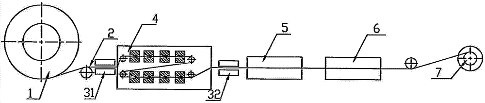
[0027] A method for processing a photovoltaic ribbon, the steps of the method are as follows:

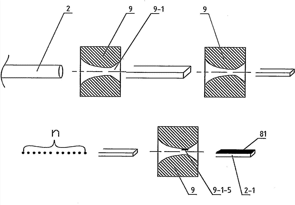
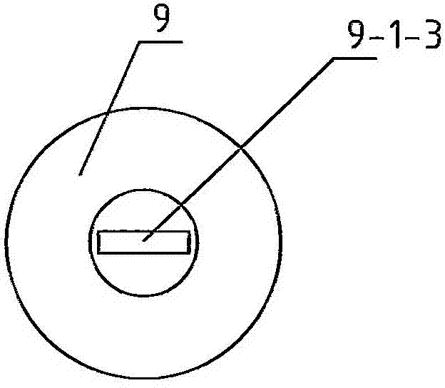
[0028] a) Provide a raw copper rod 2;

[0029] b) using the raw material copper rod 2 to form a copper strip of the required size by wire drawing through the wire drawing device 4 and forming a structure with reflective grooves on the surface of the copper strip to obtain the first semi-finished product;

[0030] c) Annealing the first semi-finished product by annealing process to form the second semi-finished product;

[0031] d) Reasonably select the coating metal, use the electroplating process to electroplate the second semi-finished product, and control the thickness of the coating to 1μm~30μm to obtain the required photovoltaic ribbon.

[00...


PUM

PropertyMeasurementUnit
thicknessaaaaaaaaaa
thicknessaaaaaaaaaa

Abstract

The invention discloses a processing method for photovoltaic solder strips and a wire-drawing die and a photovoltaic solder strip processing device used in the method. The method comprises the following steps: a) providing a raw material copper bar; b) carrying out wire-drawing forming on the raw material copper bar through a wire-drawing device, so that a copper strip with a required size is formed, and the surface of the copper strip is formed into a structure with a reflective groove, thereby obtaining a first semi-finished product; c) carrying out annealing treatment on the first semi-finished product by using an annealing process so as to form a second semi-finished product; and d) reasonably selecting a coating metal, and carrying out electroplating treatment on the second semi-finished product by using an electroplating process, and controlling the thickness of the coating to be 1-30 mu m, thereby obtaining a required photovoltaic solder strip. By using the method, a reflective groove can be formed on the surface of a photovoltaic solder strip, so that the optical utilization rate of the photovoltaic solder strip and the power of a solar energy assembly are increased; the method improves the dimensional stability and production efficiency of photovoltaic solder strips, increases the reflective effect of photovoltaic solder strips, reduces the production cost of photovoltaic solder strips, and optimizes the process steps.

Description

technical field [0001] The invention relates to a processing method of a photovoltaic welding ribbon, a wire drawing die used therefor and a photovoltaic welding ribbon processing equipment, belonging to the technical field of photovoltaic welding ribbon processing. Background technique [0002] At present, photovoltaic ribbon is the key auxiliary material for connecting solar cells into strings in solar module systems. Solar cells are connected through photovoltaic ribbons to form a complete electrical path. Light energy is converted into electrical energy through solar cells, and the generated current is passed through photovoltaic soldering The belt forms a transmission circuit and provides a pathway basis for utilizing solar energy. The surface of ordinary solder ribbon is relatively flat after drying, and the light entering the component is incident on the flat ribbon surface, and reflected by the mirror surface cannot be used. There are also some special special-shape...

Claims


Application Information

Patent Timeline
Patent Type & Authority Applications(China)
IPC IPC(8): B21C1/04B21C3/02C25D7/06
Inventor 陈辉张舒杨泽民
Owner TRINA SOLAR CO LTD
Why Eureka
Try Eureka