Improved structure for cmos etsoi with multiple threshold voltages and active well bias capability

A biasing and insulating layer technology, applied in the direction of electric solid-state devices, circuits, electrical components, etc., can solve the problems of random doping fluctuations, increased drain leakage, etc.

Active Publication Date: 2014-01-29
GLOBALFOUNDRIES INC
View PDF6 Cites 2 Cited by
  • Summary
  • Abstract
  • Description
  • Claims
  • Application Information

AI Technical Summary

Problems solved by technology

Although halo implants control short channel effects, they also lead to large random doping fluctuations, increasing junction leakage and gate-induced drain leakage (GIDL), which is fatal for low-power platforms

Method used


Image

  • Improved structure for cmos etsoi with multiple threshold voltages and active well bias capability
  • Improved structure for cmos etsoi with multiple threshold voltages and active well bias capability
  • Improved structure for cmos etsoi with multiple threshold voltages and active well bias capability

Examples


Embodiment Construction

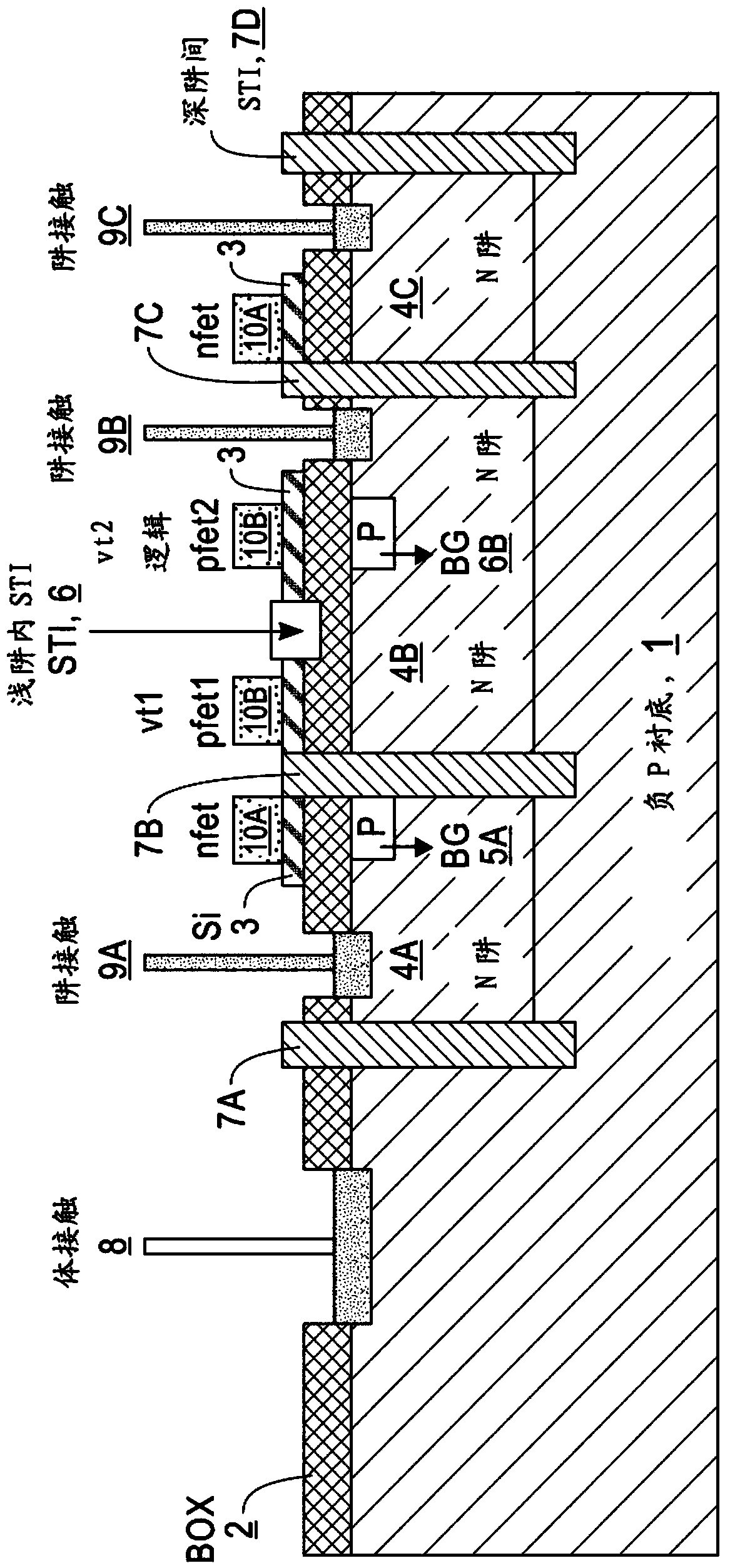
[0015] Overall, it may be advantageous to use different back gate doping types (p-type or n-type) to achieve the desired transistor threshold voltage. Basically, two different threshold voltages are achieved using two different doping types. Changing the back gate type from n-type to p-type results in a change in work function of about one volt, which is electrically equivalent to changing the applied potential by that amount. Using a different doping of the back gate may be simpler to implement than modifying the work function of the top gate and can reduce the number of masks required. Additionally, different back gates can be used for other functions.

[0016] It may also be beneficial to apply different back gate biases to nFETs and pFETs in order to tune performance, compensate for process variations and optimize a given front gate work function.

[0017] It may also be advantageous to apply the same backgate bias to all NFETs and the same backgate bias to all PFETs in ...


PUM


Abstract

A semiconductor substrate having a first type of conductivity and a top surface, a layer of oxide disposed over the top surface and a semiconductor layer disposed over the layer of oxide. A plurality of transistor devices are disposed upon the semiconductor layer. Each transistor device includes a channel between a source and a drain, where some transistor devices have a first type of channel conductivity and the remaining transistor devices have a second type of channel conductivity. A well region is formed adjacent to the top surface. The well region has a second type of conductivity. First trench isolation regions are between adjacent transistor devices that extend through the semiconductor layer. Second trench isolation regions are between adjacent transistor devices of opposite channel conductivity.

Description

technical field [0001] Exemplary embodiments of the present invention relate generally to semiconductor devices and fabrication techniques, and more particularly to utilizing extremely thin silicon-on-insulator (ETSOI) substrates to fabricate semiconductor transistor devices, such as those used in static random access memory (SRAM) and related Semiconductor transistor devices in logic circuits. Background technique [0002] In silicon-on-insulator (SOI) technology, a thin layer of silicon is formed on an insulating layer, such as silicon oxide, which is formed on a substrate. This insulating layer is often referred to as a buried oxide (BOX) layer or simply BOX. For a single BOX SOI wafer, the thin silicon layer is divided into active regions by shallow trench isolation (STI) that intersects the BOX and provides total isolation for the active device areas formed in the silicon layer. For example, by ion-implanting n-type and / or p-type dopant materials into a thin silicon l...

Claims


Application Information

Patent Timeline
Patent Type & Authority Applications(China)
IPC IPC(8): H01L27/11H01L21/8244H01L27/12
CPCH01L21/823878H01L21/84H01L27/1203H01L21/823892
Inventor R.H.邓纳德T.B.胡克
Owner GLOBALFOUNDRIES INC
Why Eureka
Try Eureka