Band-gap reference voltage source design with high gain and high rejection ratio

A reference voltage source, high rejection technology, applied in the direction of regulating electrical variables, control/regulating systems, instruments, etc., can solve problems such as being susceptible to self and external noise and offset, low power supply rejection ratio of reference circuits, and low driving capability , to achieve the effect of enhancing anti-interference performance, improving power supply rejection ratio and high rejection ratio

Inactive Publication Date: 2014-02-05
CHINA UNIV OF MINING & TECH
View PDF8 Cites 16 Cited by
  • Summary
  • Abstract
  • Description
  • Claims
  • Application Information

AI Technical Summary

Problems solved by technology

[0006] The present invention can solve the problems of low power supply rejection ratio of existing reference circuits, susceptibility to self and external noise and offset, low drive capability, narrow frequency band, low phase margin, etc.

Method used


Image

  • Band-gap reference voltage source design with high gain and high rejection ratio
  • Band-gap reference voltage source design with high gain and high rejection ratio
  • Band-gap reference voltage source design with high gain and high rejection ratio

Examples


Embodiment Construction

[0023] In order to make the technical problems, technical solutions and beneficial effects solved by the present invention clearer, the present invention will be further described in detail below in conjunction with the accompanying drawings and embodiments. It should be understood that the specific embodiments described here are only used to explain the present invention, not to limit the present invention.

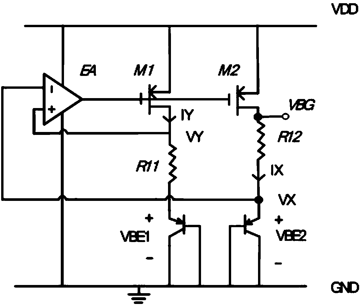
[0024] The invention designs a bandgap reference voltage source with high gain and high rejection ratio.

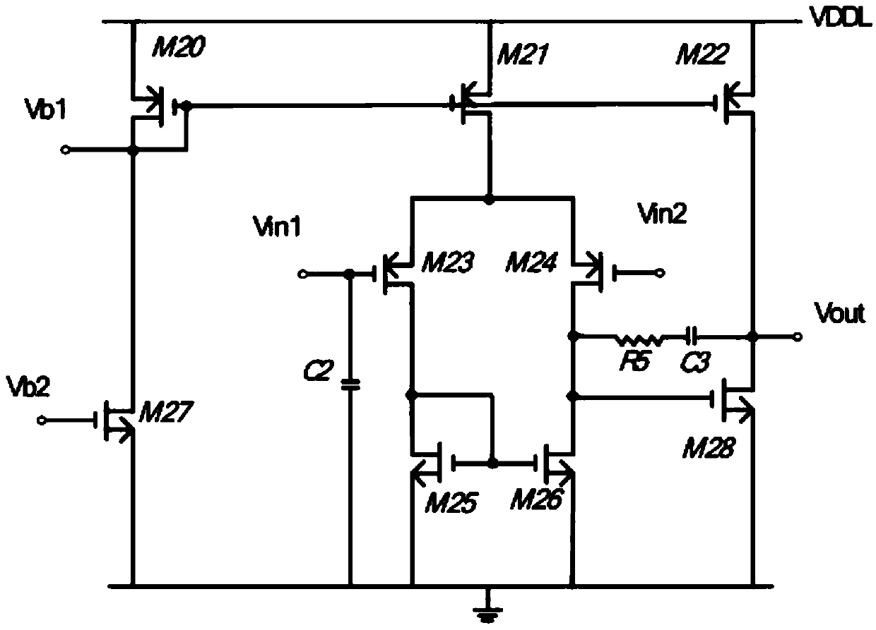
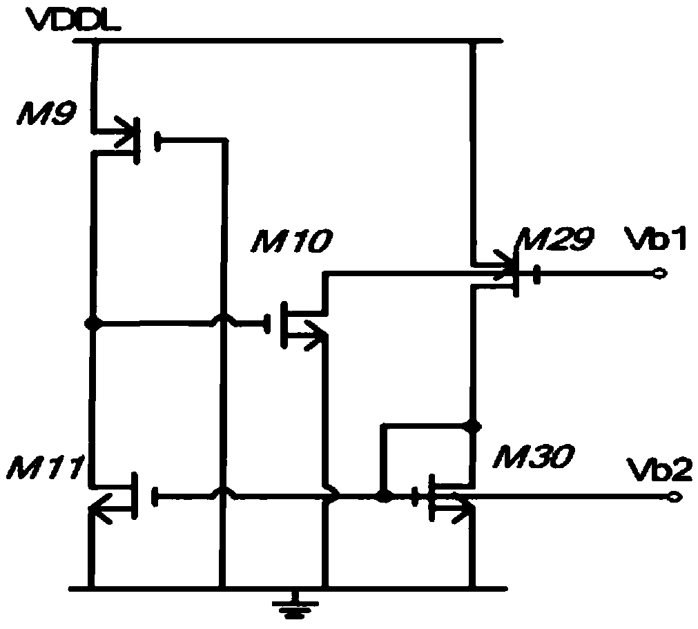
[0025] refer to figure 2 , the operational amplifier circuit used in this design, such as figure 2 , the operational amplifier circuit adopts the form of double-ended input and single-ended output, and is composed of PMOS transistors M20-M24, NMOS transistors M25-M28, a fifth resistor R5, a second capacitor C2, and a third capacitor C3; the PMOS transistor M20 The source of ~M22 is connected to the participating voltage source VDDL, the gate is connected to the...


PUM


Abstract

The invention provides a band-gap reference voltage source design with high gain and a high rejection ratio. A band-gap reference voltage source circuit is composed of an operational amplifier circuit, a starting and biasing circuit, a rejection ratio increasing circuit and the band-gap reference voltage source circuit. A high-gain operational amplifier is adopted for effectively guaranteeing precision and stability of Delta VBE, and offset is reduced by means of multistage amplification; the starting and biasing circuit provides starting voltage and bias for the other circuits, and is closed after the other circuits are started; the rejection ratio increasing circuit increases rejection of the whole circuit on power supply change in a current feedback mode, a locally supplied power supply VDDL is generated, and anti-interference performance of the circuit is enhanced; the band-gap reference voltage source circuit increases the power supply rejection ratio of output voltage by adoption of a current mirror of a self-bias cascade structure, and coordinates with an external circuit to generate reference voltage with stable performance and zero-temperature coefficient. Due to the adoption of the high-gain two-stage operational amplifier, a voltage source isolation technique, an RC compensation network and the current mirror in the self-bias cascade structure, the circuit has low offset voltage, high phase margin, high gain and high rejection ratio, and impact caused by MOS (metal oxide semiconductor) device channel modulation effect is reduced.

Description

technical field [0001] The invention relates to the technical field of integrated circuits, in particular to a design of a bandgap reference voltage source with high gain and high rejection ratio. Background technique [0002] In the field of analog integrated circuit or mixed signal design, the reference voltage source is a very important module, and the reference voltage source occupies a pivotal position in the DAC circuit, and its design directly affects the accuracy and stability of the DAC output. In the design of the bandgap reference voltage source, the selection of the operational amplifier circuit is very important. Its open-loop gain and input offset directly determine the output accuracy and stability of the bandgap reference voltage source. In order to reduce the influence of the offset on the reference voltage, the operation The offset should be as small as possible. And temperature changes, fluctuations in current and voltage, and manufacturing process deviat...

Claims


Application Information

Patent Timeline
Patent Type & Authority Applications(China)
IPC IPC(8): G05F1/56
Inventor 刘海崔海娜潘洪帅牛晓聪程雪荆胜羽程德强
Owner CHINA UNIV OF MINING & TECH
Why Eureka
Try Eureka