

An Optical Proximity Correction Method
A technology of optical proximity and photolithography, applied in optics, optomechanical equipment, originals for optomechanical processing, etc., can solve the problems of product quality, impact on circuit performance, time-consuming and easy to miss
- Summary
- Abstract
- Description
- Claims
- Application Information
AI Technical Summary
Problems solved by technology
Method used
Image


Examples
Embodiment Construction
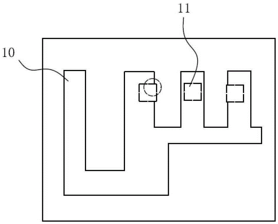
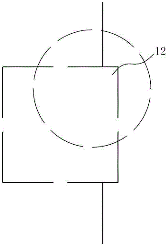
[0029] As mentioned in the background art, because in the An (metal wiring level), in order to cover holes used as conductive plugs, some metal lines may have bumps. In the existing OPC optimization processing program, there is no step of judging whether these protrusions are useful structures, so after the OPC optimization is completed, defects are often formed in these protrusions, and these defects not only destroy the metal The structural characteristics of the line itself, and on the contrary, further expose the place that originally needs to cover the hole, which seriously affects the quality of the device. Therefore, it is necessary to optimize the existing optical proximity correction method to avoid these defects and improve the quality of semiconductor devices.
[0030] The present invention aims at the above problems. In the existing OPC program, a cleaning program for the protrusions caused by covering holes is added. Before the OPC processing program is executed, ...
PUM
 Abstract
Description
Claims
Application Information