Photoetching method for photoresist as silicon groove etching mask

A technology for etching masks and photoresists, which is applied in the field of semiconductor technology and can solve problems such as silicon corrosion

Active Publication Date: 2014-02-12
CSMC TECH FAB2 CO LTD
View PDF6 Cites 8 Cited by
  • Summary
  • Abstract
  • Description
  • Claims
  • Application Information

AI Technical Summary

Problems solved by technology

[0004] Based on this, it is necessary to provide a photoresist as a silicon groove etching mask for the problem that part of the silicon covered by the photoresist will also be corroded when the photoresist is used as a mask for deep silicon groove etching. photolithography method

Method used


Image

  • Photoetching method for photoresist as silicon groove etching mask

Examples


Embodiment Construction

[0016] In order to make the objectives, features, and advantages of the present invention more obvious and understandable, the specific embodiments of the present invention will be described in detail below with reference to the accompanying drawings.

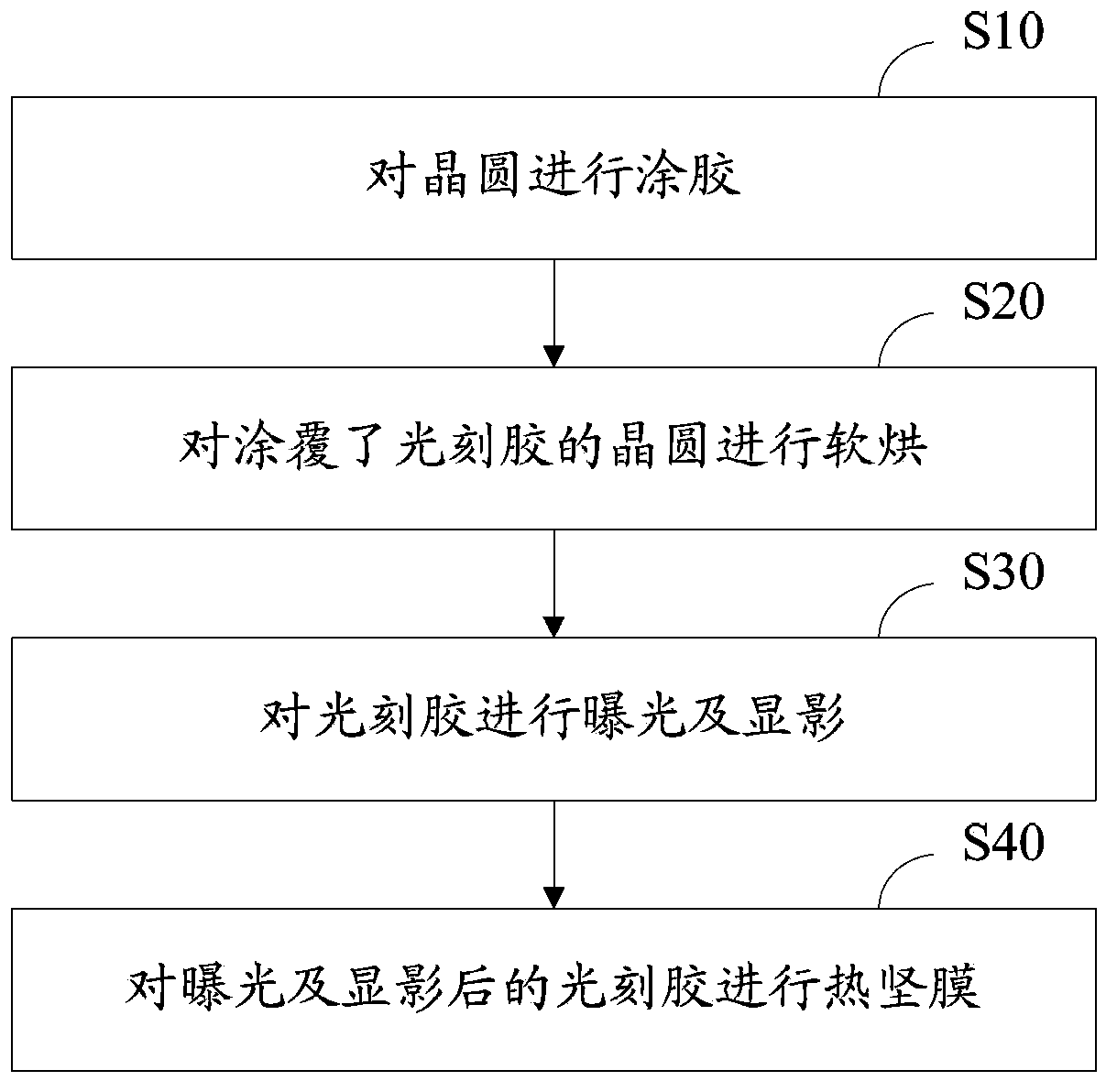
[0017] figure 1 It is a flowchart of a photolithography method of photoresist used as a silicon trench etching mask in an embodiment, including the following steps:

[0018] S10: Glue the wafer.

[0019] Before applying the adhesive, a layer of hexamethyldisilazane (HMDS) or other compounds that can enhance the adhesion between the photoresist and the wafer can be applied to the surface of the wafer. The photoresist is sprayed on the surface of the wafer, and then a layer of photoresist of the expected thickness is obtained by spin-off.

[0020] S20, soft-bake the wafer coated with photoresist.

[0021] Soft bake can volatilize part of the solvent in the photoresist and enhance the adhesion of the photoresist.

[0022] S30, exposing and...


PUM

PropertyMeasurementUnit
thicknessaaaaaaaaaa

Abstract

A photoetching method for a photoresist as a silicon groove etching mask comprises the following steps: gluing a wafer; performing soft baking on the wafer coated with the photoresist; performing exposure and development on the photoresist; performing hardening on the photoresist subjected to exposure and development, wherein the thickness of the photoresist on the wafer after the hardening step is finished is 7.2-7.8 mu m; and performing etching on a silicon groove by taking the hardened photoresist as the mask. The photoetching method does not comprise the step of performing optical stabilization processing on the photoresist. By forming the thick glue with a thickness large than 7 mu m, the selectivity ratio of silicon is improved. Also because the photoetching method does not comprises the step of performing optical stabilization processing on the photoresist, a dry-process glue-removing technology can be used, and thus a spin-dry step is not needed after the glue is removed, and the problem of fragments caused by spin dry is avoided.

Description

Technical field [0001] The invention relates to a semiconductor process, in particular to a photolithography method of photoresist used as a silicon trench etching mask. Background technique [0002] SiO is usually used for silicon trench etching 2 , SiN and other media are used as hardmasks, which can solve the normal etching problems of several μm to more than ten μm. But for MEMS microphone products, it is necessary to etch a 300μm deep silicon groove on the thin sheet (380μm thickness). If using SiO 2 The other medium is used as a hard mask, and the silicon is also corroded when the mask is removed by dry method, which affects the shape of the silicon groove. If the mask is removed by a wet method, it needs to be dried afterwards, and the thin slices that have formed deep silicon grooves are easily broken. [0003] Based on this, the inventor tried to use an in-line 4.8 μm thick photoresist as a barrier layer for etching. However, during use, it is found that the choice of s...

Claims


Application Information

Patent Timeline
Patent Type & Authority Applications(China)
IPC IPC(8): G03F7/00G03F7/16H01L21/027
Inventor 徐春云
Owner CSMC TECH FAB2 CO LTD
Why Eureka
Try Eureka