Supercharge Your Innovation With Domain-Expert AI Agents!

Structure and manufacturing method of photolithography alignment mark for comprehensive silicon epitaxial process

A lithography alignment and silicon epitaxy technology, used in semiconductor/solid-state device manufacturing, electrical components, electrical solid-state devices, etc., can solve problems such as deformation and disappearance of lithography alignment marks

Active Publication Date: 2016-06-08
SHANGHAI HUAHONG GRACE SEMICON MFG CORP
View PDF4 Cites 0 Cited by
  • Summary
  • Abstract
  • Description
  • Claims
  • Application Information

AI Technical Summary

Problems solved by technology

[0003] One of the technical problems to be solved by the present invention is to provide a method for making a comprehensive silicon epitaxial process lithography alignment mark, which can solve the problem of deformation and disappearance of the lithography alignment mark after epitaxial growth

Method used


Image

  • Structure and manufacturing method of photolithography alignment mark for comprehensive silicon epitaxial process
  • Structure and manufacturing method of photolithography alignment mark for comprehensive silicon epitaxial process
  • Structure and manufacturing method of photolithography alignment mark for comprehensive silicon epitaxial process

Examples


Embodiment Construction

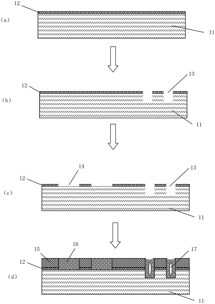
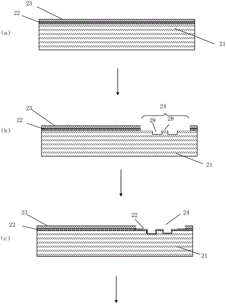
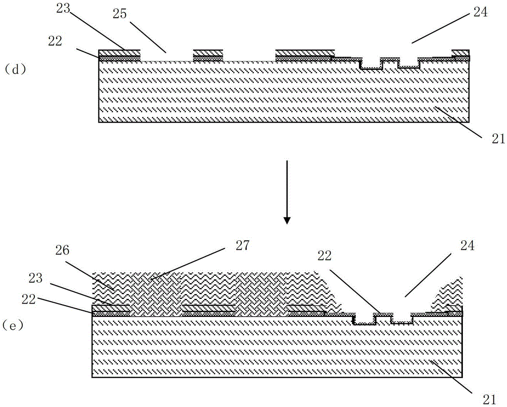
[0029] In order to have a more specific understanding of the technical content, characteristics and effects of the present invention, now in conjunction with the illustrated embodiment, the details are as follows:

[0030] The selective silicon epitaxy process refers to the growth of a single crystal on a silicon single crystal by adding a precursor containing chlorine atoms to the silicon source during the silicon epitaxial growth process, but not on a certain dielectric film. . Different dielectric films require different components of chlorine-containing precursors. Therefore, when multiple dielectric films exist on the same surface at the same time, silicon epitaxy can be grown on a certain dielectric film under a specific chlorine-containing precursor component. , while silicon epitaxy does not grow on other dielectric films.

[0031] Utilizing the characteristics of the above-mentioned selective silicon epitaxial process, the present invention has produced the lithograp...


PUM

PropertyMeasurementUnit
thicknessaaaaaaaaaa

Abstract

The invention discloses a method for making a photolithographic alignment mark in a comprehensive silicon epitaxy process, which comprises the steps of: 1) growing first and second dielectric films sequentially on a silicon substrate; wherein, the first dielectric film is capable of blocking silicon The film layer of crystal growth; the second dielectric film is a film layer that can prevent the growth of the first dielectric film on its surface; 2) etching out the lithography alignment window and lithography alignment groove; 3) in the lithography alignment Window and lithography are aligned with the surface of the trench to grow the first dielectric film; 4) Etching out the silicon single crystal window; 5) Full-scale silicon epitaxial growth. The invention also discloses the structure of the photolithographic alignment mark manufactured by the method. The invention forms a non-deposition area on the surface of the photolithographic alignment mark by adjusting the epitaxial deposition program, and solves the problem of deformation and disappearance of the alignment mark after epitaxial growth.

Description

technical field [0001] The invention relates to the field of semiconductor integrated circuit manufacturing, in particular to a structure and a manufacturing method of a photolithographic alignment mark in a comprehensive silicon epitaxy process. Background technique [0002] The comprehensive silicon epitaxy process refers to the presence of semiconductor regions and dielectric film regions on the semiconductor surface. The silicon epitaxy process grows silicon single crystals in the semiconductor region, and grows silicon polycrystalline or silicon amorphous in the dielectric film region. The fabrication method of conventional full-scale silicon epitaxial process lithography alignment mark is (see figure 1 ): (1) growing a dielectric film 12 on a silicon substrate 11, such as figure 1 As shown in (a); (2) etching a photolithographic alignment groove 13, such as figure 1 As shown in (b); (3) etching out the single crystal window 14, such as figure 1 As shown in (c); (4) ...

Claims


Application Information

Patent Timeline
Patent Type & Authority Patents(China)
IPC IPC(8): H01L21/31H01L23/544
Inventor 刘继全高杏
Owner SHANGHAI HUAHONG GRACE SEMICON MFG CORP
Features
  • R&D
  • Intellectual Property
  • Life Sciences
  • Materials
  • Tech Scout
  • Unparalleled Data Quality
  • Higher Quality Content
  • 60% Fewer Hallucinations
Learn More