A semiconductor structure, a doping method thereof, and a method for forming a fin field effect transistor

A fin field effect transistor and semiconductor technology, which is applied in semiconductor devices, semiconductor/solid-state device manufacturing, electrical components, etc., can solve problems such as uneven doping concentration, and achieve the effects of uniform doping concentration and simple process

Inactive Publication Date: 2014-02-19
SEMICON MFG INT (SHANGHAI) CORP
View PDF6 Cites 14 Cited by
  • Summary
  • Abstract
  • Description
  • Claims
  • Application Information

AI Technical Summary

Problems solved by technology

[0004] In the prior art, the source / drain region of the fin field effect transistor located at the fin is usually doped by ion implantation, but the doping method of ion implantation will cause different doping concentrations in different regions of the source / drain. uniform

Method used


Image

  • A semiconductor structure, a doping method thereof, and a method for forming a fin field effect transistor
  • A semiconductor structure, a doping method thereof, and a method for forming a fin field effect transistor
  • A semiconductor structure, a doping method thereof, and a method for forming a fin field effect transistor

Examples


Embodiment Construction

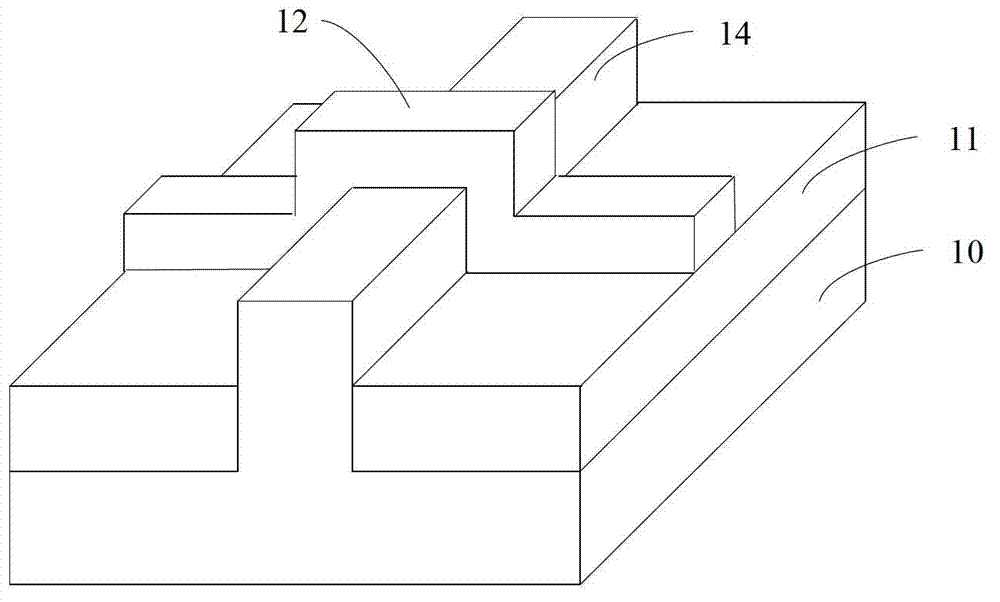
[0031] It can be seen from the background technology that in the prior art solutions, the source / drain regions of the fin field effect transistors located in the fins are usually doped by ion implantation, but because the source / drain regions of the fin field effect transistors As a three-dimensional structure, the angle of ion implantation is different, and the concentration of ion implantation in the source / drain region will be different. Therefore, the doping method of ion implantation will cause uneven doping concentration in different regions of the source / drain region of the FinFET, which is non-conformal doping.

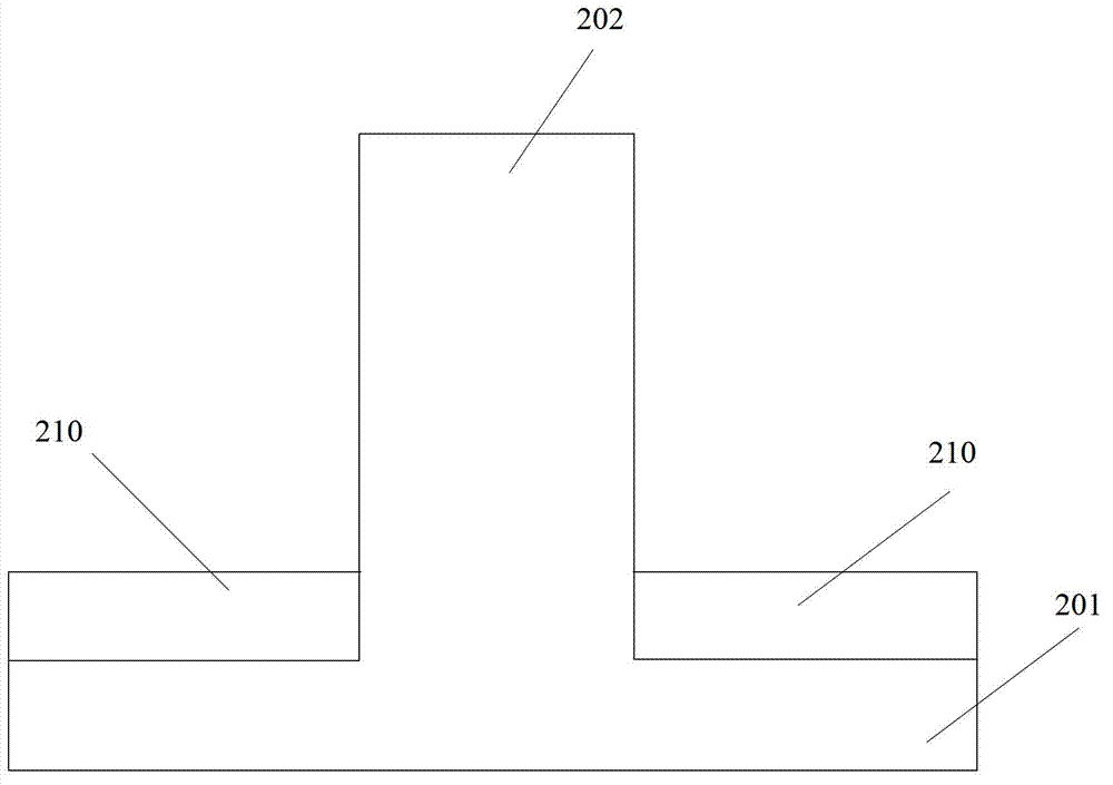
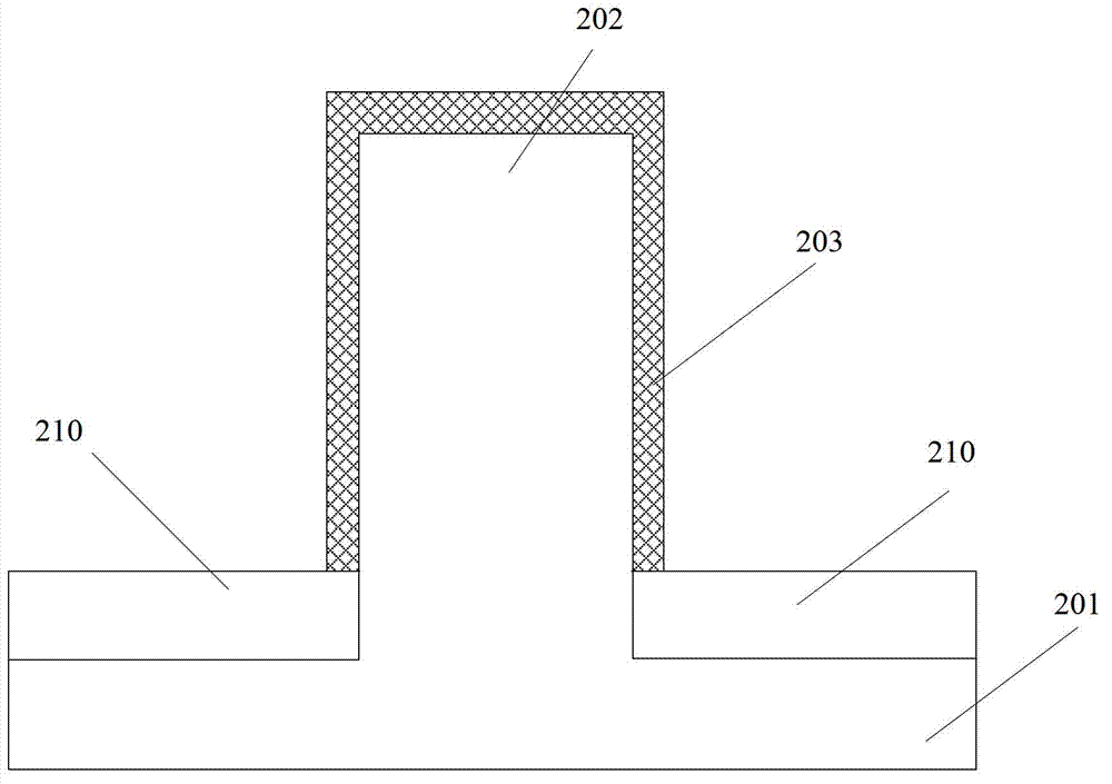
[0032] In order to solve the above problems, the inventors of the present invention provide a method for doping a semiconductor structure, including: providing a semiconductor substrate having fins on the semiconductor substrate; forming an impurity layer on the surface of the fin; forming a capping layer on the surface of the impurity layer, and the capping l...


PUM

PropertyMeasurementUnit
thicknessaaaaaaaaaa
thicknessaaaaaaaaaa
thicknessaaaaaaaaaa

Abstract

Provided are a semiconductor structure, a doping method thereof, and a method for forming a fin field effect transistor. The doping method of the semiconductor structure comprises: providing a semiconductor substrate on which a fin portion is disposed; forming an impurity layer on the surface of the fin portion; forming a cover cap layer on the surface of the impurity layer, wherein the cover cap layer comprises an amorphous carbon layer; annealing the formed impurity layer and the cover cap layer in order to put the impurity layer into the fin portion; and removing the cover cap layer. The semiconductor structure and the fin field effect transistor are uniformly doped and have simple techniques.

Description

technical field [0001] The invention relates to the field of semiconductor manufacturing, in particular to a semiconductor structure and its doping method, and a method for forming a fin field effect transistor. Background technique [0002] MOS transistors generate switching signals by applying a voltage to the gate to adjust the current through the source and drain regions. However, when the semiconductor technology enters the node below 30 nanometers, the traditional planar MOS transistor has a weak ability to control the channel current, resulting in serious leakage current. Fin Field Effect Transistor (Fin FET) is an emerging multi-gate device, which generally includes a semiconductor fin with a high aspect ratio, in which the channel region and source / drain region of the transistor are formed, and in part of the fin The gate is formed on the top and outside the sidewalls of the portion. [0003] figure 1 A schematic diagram of a three-dimensional structure of a fin ...

Claims


Application Information

Patent Timeline
Patent Type & Authority Applications(China)
IPC IPC(8): H01L21/225H01L29/423H01L29/78H01L21/28H01L21/336
CPCH01L29/66803H01L21/0257H01L29/0847H01L29/66795H01L29/7856
Inventor 三重野文健
Owner SEMICON MFG INT (SHANGHAI) CORP
Why Eureka
Try Eureka