Manufacturing method of integrated Schottky split-gate type power MOS device

A technology of MOS devices and split gates, which is applied in semiconductor/solid-state device manufacturing, semiconductor devices, electrical components, etc., can solve problems such as complex manufacturing processes, and achieve the effects of process simplification, low on-resistance, and increased switching speed

Inactive Publication Date: 2014-02-19
HARBIN ENG UNIV
View PDF6 Cites 7 Cited by
  • Summary
  • Abstract
  • Description
  • Claims
  • Application Information

AI Technical Summary

Problems solved by technology

[0007] The invention proposes a manufacturing method of an integrated Schottky split-gate power MOS device, which is used to solve the problem of complex manufacturing process in the prior art

Method used


Image

  • Manufacturing method of integrated Schottky split-gate type power MOS device
  • Manufacturing method of integrated Schottky split-gate type power MOS device
  • Manufacturing method of integrated Schottky split-gate type power MOS device

Examples


Embodiment Construction

[0027] The implementation of the present invention will be described below in conjunction with the accompanying drawings.

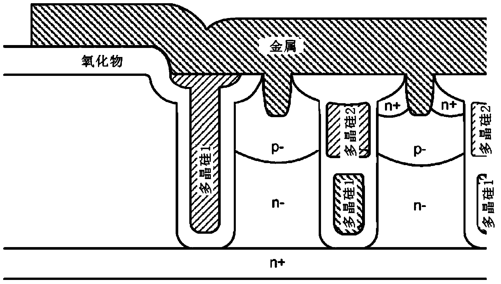
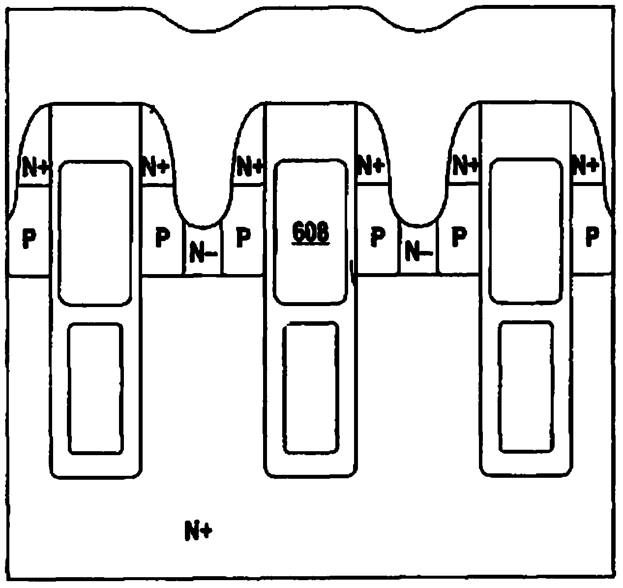
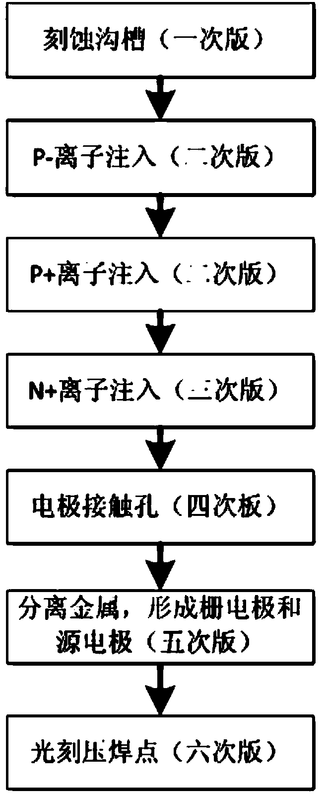
[0028] In the embodiment of the present invention, six photolithography plates are used to realize the layout and process design of an integrated Schottky split gate power MOS device, and the N+ region, the P+ region and the Schottky contact region in the source electrode of the device are respectively drawn out and Shorting, the proportion of Schottky contact in the source electrode is not affected by the trench spacing, which can optimize the performance of the designed device. The whole process requires six plates, and the process is simplified accordingly. While ensuring the ultra-low on-resistance of the device, it does not affect the breakdown voltage of the device. Schottky is integrated in the device cell, and the switching rate of the device is increased, and the utilization rate of the silicon chip is also improved.

[0029] An embodiment of th...


PUM


Abstract

The invention discloses a manufacturing method of an integrated Schottky split-gate type power MOS device. The integrated Schottky split-gate type power MOS device is manufactured by utilizing 6 mask templates. Compared with a traditional manufacturing process of a split-gate type channel power MOS device, the manufacturing method of the integrated Schottky split-gate type power MOS device can reduce process steps and process difficulty.

Description

technical field [0001] The invention relates to the field of semiconductors, in particular to a method for manufacturing an integrated Schottky split gate power metal oxide semiconductor (METAL-OXIDE-SEMICONDUCTOR, MOS) device. Background technique [0002] In the 1990s, the main research direction of the development and industrialization technology of power trench metal oxide semiconductor MOS field effect transistor (Power Trench MOSFET) was mainly to minimize the forward conduction resistance (Ron) of low voltage power devices. Today, the structure of power trench MOS devices has been applied to most power metal-oxide-semiconductor field-effect transistors (METAL-OXIDE-SEMICONDUCTOR FIELD-EFFECT TRANSISTOR, MOSFET) applications, and the characteristics of the device are constantly approaching a silicon material dimension constraints. The proposal of REduced SURface Field (RESURF) technology can make power trench MOS devices with a breakdown voltage of 600V exceed the one...

Claims


Application Information

Patent Timeline
Patent Type & Authority Applications(China)
IPC IPC(8): H01L21/336
CPCH01L29/66848H01L21/28H01L29/401
Inventor 王颖胡海帆曹菲刘云涛
Owner HARBIN ENG UNIV
Why Eureka
Try Eureka