Chemical etching transfer method for CVD epitaxial growth of graphene based on Gan substrate

A transfer method and epitaxial growth technology, applied in chemical instruments and methods, single crystal growth, crystal growth, etc., can solve the problems of poor corrosion effect, degradation of graphene electrical properties, increase of corrosion time, etc., and reduce the corrosion temperature , to avoid adverse effects, to reduce the effect of corrosion time

Active Publication Date: 2016-01-13
XIDIAN UNIV
View PDF5 Cites 0 Cited by
  • Summary
  • Abstract
  • Description
  • Claims
  • Application Information

AI Technical Summary

Problems solved by technology

However, because the non-graphene contact surface is attached to other substrates, and the other side is covered by graphene, only the metal side is in contact with the corrosion solution, the effective contact surface is extremely small, the corrosion time is greatly increased, and the corrosion effect is significantly worse. , so that the electrical properties of graphene degrade

Method used


Image

  • Chemical etching transfer method for CVD epitaxial growth of graphene based on Gan substrate
  • Chemical etching transfer method for CVD epitaxial growth of graphene based on Gan substrate

Examples


Embodiment 1

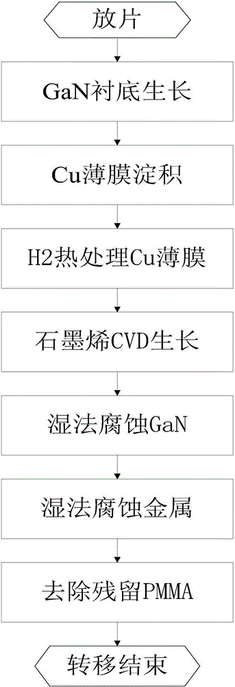
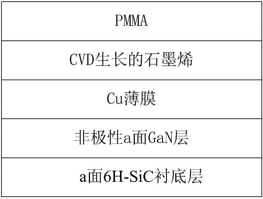
[0025] Step 1, growing a GaN substrate.

[0026] Place the a-side silicon carbide 6H-SiC substrate in the metal organic chemical vapor deposition MOCVD reaction chamber, and pass the mixed gas of gallium source and ammonia gas into the reaction chamber, the flow rate of gallium source is 50 μmol / min, and the flow rate of ammonia gas is 1000 sccm , continued for 1 hour, and grew an a-plane GaN substrate with a thickness of 1 μm.

[0027] Step 2, Cu film deposition and annealing treatment.

[0028] Vacuumize the reaction chamber to ensure that the air pressure is not higher than 10 -6 Under the condition of Torr, a Cu film with a thickness of 1 μm was deposited on the GaN substrate by electron beam evaporation, and H2 with a flow rate of 1 sccm was introduced into the reaction chamber, and the temperature in the reaction chamber was raised to 900 ° C, and the deposited Cu film was thermally annealed. The annealing time is 20min.

[0029] Step 3, growing graphene.

[0030] It...

Embodiment 2

[0045] Step A, growing a GaN substrate.

[0046] Place the a-side silicon carbide 6H-SiC substrate in the metal organic chemical vapor deposition MOCVD reaction chamber, and feed the mixed gas of gallium source and ammonia gas into the reaction chamber. The flow rate of gallium source is 100 μmol / min, and the flow rate of ammonia gas is 2000 sccm , continued for 40 hours, and grew an a-plane GaN substrate with a thickness of 2 μm.

[0047] Step B, Cu film deposition and annealing treatment.

[0048] Vacuumize the reaction chamber to ensure that the air pressure is not higher than 10 -6 Under the condition of Torr, electron beam evaporation deposits a Cu film with a thickness of 2 μm on the GaN substrate, feeds H2 with a flow rate of 10 sccm into the reaction chamber, raises the temperature in the reaction chamber to 950 ° C, and performs thermal annealing on the deposited Cu film. The annealing time is 20min.

[0049] Step C, growing graphene.

[0050] It is 50sccm H that ...

Embodiment 3

[0065] Step 1, growing a GaN substrate.

[0066] Place the a-side silicon carbide 6H-SiC substrate in the metal organic chemical vapor deposition MOCVD reaction chamber, feed the mixed gas of gallium source and ammonia gas into the reaction chamber, the flow rate of gallium source is 150 μmol / min, and the flow rate of ammonia gas is 3000 sccm , continued for 0.5 hours, and grew an a-plane GaN substrate with a thickness of 1.5 μm.

[0067] Step 2, Cu film deposition and annealing treatment.

[0068] Vacuumize the reaction chamber to ensure that the air pressure is not higher than 10 -6 Under the condition of Torr, electron beam evaporation deposits a Cu film with a thickness of 3 μm on the GaN substrate, feeds H2 with a flow rate of 20 sccm into the reaction chamber, raises the temperature in the reaction chamber to 1000 ° C, and performs thermal annealing on the deposited Cu film. The annealing time is 60min.

[0069] Step three, grow graphene.

[0070] It is 100sccm H2 th...


PUM


Abstract

The invention discloses a chemical corrosion transfer method based on GaN substrate CVD epitaxial growth graphene. The problems that a copper substrate is wasted, and graphene transfer wastes time in the prior art are mainly solved. The chemical corrosion transfer method comprises the implementation steps that (1), a-face silicon carbide is arranged in an MOCVD reaction chamber, a gallium source and ammonia gas are filled into the MOCVD reaction chamber, and a-face GaN is grown; (2), a Cu thin film is deposited on the GaN through electron beam evaporation; (3), H2 is filled into the MOCVD reaction chamber, and thermal annealing is carried out on the Cu thin film; (4), H2 and CH4 are filled into the MOCVD reaction chamber, and the graphene is grown through chemical meteorology deposition; (5), the surface of the graphene is coated with photoresist in a spinning mode, the graphene is placed in potassium oxide solutions, a GaN middle layer is accelerated to be corroded with the help of lasers, and then the lower Cu thin film is corroded and removed; (6), the photoresist of the graphene with the thin film corroded and removed is upwards placed in an insulation substrate, the graphene is heated after being dried through air, then the graphene is cooled to indoor temperature and is placed in acetone to remove the photoresist on the upper surface of the graphene, and graphene transfer is achieved. The chemical corrosion transfer method has the advantages of being short in transfer time and saving the Cu substrate.

Description

technical field [0001] The invention belongs to the field of microelectronics technology, and relates to a method for manufacturing and transferring graphene, in particular to a method for growing graphene based on chemical vapor deposition CVD epitaxial growth of a gallium nitride (GaN) substrate and transferring graphene by chemically corroding a substrate , which can be used for the growth and transfer of graphene materials in CVD epitaxy equipment. technical background [0002] Graphene is a carbon-based two-dimensional crystal with excellent physical and chemical properties. Two-dimensional electron density on graphene surface reaches 10 13 cm -2 , the mobility of electrons exceeds 200,000 cm 2 V -1 the s -1 , electron saturation drift speed up to 10 8 cms -1 . Due to these excellent electrical properties, graphene has the potential to manufacture ultra-high-speed electronic devices. In 2010, IBM successfully developed a graphene FET with the highest frequency e...

Claims


Application Information

Patent Timeline
Patent Type & Authority Patents(China)
IPC IPC(8): H01L21/205C30B25/02C30B25/18C30B29/02
CPCC30B25/02C30B25/18C30B25/186C30B29/02H01L21/02527H01L21/0262H01L21/02694H01L21/7813
Inventor 王东闫景东宁静韩砀柴正张进成郝跃
Owner XIDIAN UNIV
Why Eureka
Try Eureka