Phosphorus doping silicon wafer, manufacturing method of phosphorus doping silicon wafer, solar cell and manufacturing method of solar cell

A technology for solar cells and solar cells, applied in the field of solar cells, can solve the problems of reducing the lifetime of carriers, being disadvantageous, reducing the recombination rate of carriers, etc., achieving a smooth distribution curve of impurity phosphorus concentration gradient, improving conversion efficiency, The effect of good electrical parameters

Active Publication Date: 2014-02-26
YINGLI GRP
View PDF7 Cites 15 Cited by
  • Summary
  • Abstract
  • Description
  • Claims
  • Application Information

AI Technical Summary

Problems solved by technology

[0005] In the existing deposition and diffusion process, due to the POCl 3 with O 2 Under the same ratio, when the impurity source phosphorus oxychloride flow rate is larger, the deposition and diffusion speed is faster, and as time goes on, the phosphorus deposited on the surface of the silicon wafer diffuses into the silicon wafer substrate, and the impurities on the silicon wafer surface Phosphorus concentration gradually decreases, because the impurity source phosphorus on the surface of the silicon wafer will continue to deposit on the surface of the silicon wafer, that is, while the phosphorus diffuses into the silicon wafer, the impurity source phosphorus oxychloride is still continuously replenished in a large concentration, Therefore, the concentration gradient of impurity phosphorus near the surface of the silicon wafer is still at a relatively high level, so the concentration gradient distribution curve of impurities is relatively gentle, resulting in the existence of a "dead layer" with a large thickness, and carriers are easily recombined in this layer , which reduces the lifetime of carriers, and the smooth gradient distribution of impurities is not conducive to the rapid transport of carriers, and is not conducive to reducing the recombination rate of carriers, which affects the conversion efficiency of solar cells. Therefore, how to develop a new diffusion process has become a current research hotspot

Method used


Image

  • Phosphorus doping silicon wafer, manufacturing method of phosphorus doping silicon wafer, solar cell and manufacturing method of solar cell
  • Phosphorus doping silicon wafer, manufacturing method of phosphorus doping silicon wafer, solar cell and manufacturing method of solar cell
  • Phosphorus doping silicon wafer, manufacturing method of phosphorus doping silicon wafer, solar cell and manufacturing method of solar cell

Examples


Embodiment 1

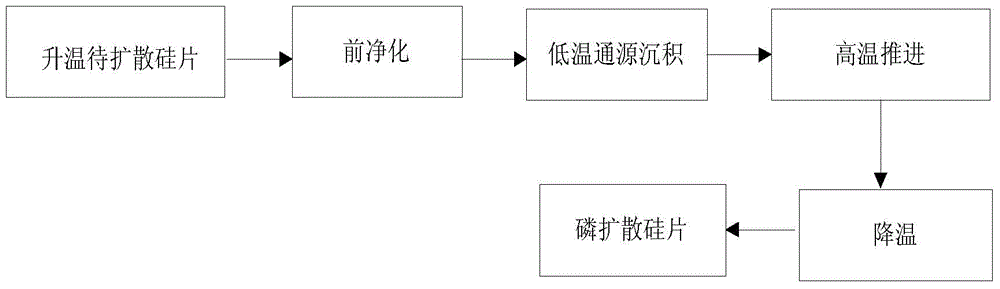
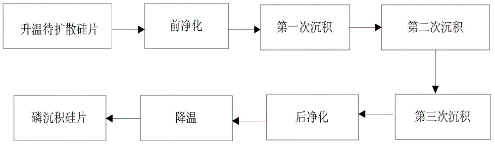
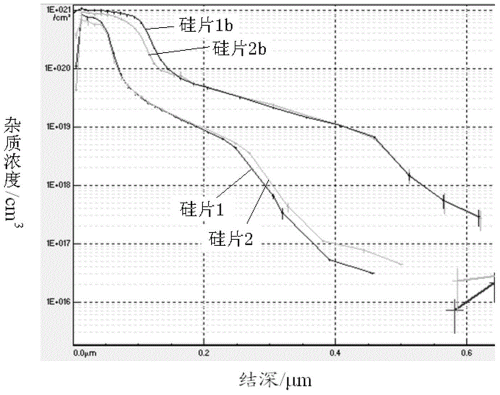
[0035] Place the P-type silicon chip in a quartz tube, raise the temperature to 860°C at 10°C / min, and pass nitrogen gas for 5 minutes while raising the temperature, with a flow rate of 8slm. After that, POCl is introduced in three steps 3 with O 2 Deposition and diffusion, where the conditions for the first step of deposition and diffusion are: POCl 3 with O 2 The total flow rate is 1600sccm, according to the volume ratio of POCl 3 :O 2 =8:1, the time of deposition and diffusion is 8 minutes; the second step of deposition and diffusion: POCl 3 with O 2 The total flow rate is 1200sccm, according to the volume ratio of POCl 3 :O 2 =5:1, the time of deposition and diffusion is 8 minutes; the third step of deposition and diffusion: POCl 3 with O 2 The total flow rate is 600sccm, by volume POCl 3 :O 2 =3:1, the deposition and diffusion time is 8 minutes. Afterwards, the temperature was lowered to room temperature at 10° C. / min, and the silicon wafer was taken out, whic...

Embodiment 2

[0037] Place the P-type silicon chip in a quartz tube, raise the temperature to 870°C at 10°C / min, and pass nitrogen gas for 2 minutes while raising the temperature, with a flow rate of 15slm. After that, POCl is introduced in three steps 3 with O 2 Deposition and diffusion, where the conditions for the first step of deposition and diffusion are: POCl 3 with O 2 The total flow rate is 1800sccm, according to the volume ratio of POCl 3 :O 2 =9:1, the time of deposition and diffusion is 5 minutes; the second step of deposition and diffusion: POCl 3 with O 2 The total flow rate is 1300sccm, by volume ratio POCl 3 :O 2 =5.5:1, the time of deposition and diffusion is 10 minutes; the third step of deposition and diffusion: POCl 3 with O 2 The total flow rate is 800sccm, according to the volume ratio of POCl 3 :O 2 =3.5:1, the deposition and diffusion time is 5 minutes. Afterwards, the temperature was lowered to room temperature at 10° C. / min, and the silicon wafer was tak...

Embodiment 3

[0039] Place the P-type silicon wafer in a quartz tube, raise the temperature to 840°C at 10°C / min, and pass nitrogen gas for 5 minutes while raising the temperature, with a flow rate of 8slm. After that, POCl is introduced in three steps 3 with O 2 Deposition and diffusion, where the conditions for the first step of deposition and diffusion are: POCl 3 with O 2 The total flow rate is 1400sccm, by volume ratio POCl 3 :O 2 =7:1, the time of deposition and diffusion is 10 minutes; the second step of deposition and diffusion: POCl 3 with O 2 The total flow rate is 1100sccm, according to the volume ratio of POCl 3 :O 2 =4.5:1, the time of deposition and diffusion is 5 minutes; the third step of deposition and diffusion: POCl 3 with O 2 The total flow rate is 600sccm, by volume POCl 3 :O 2 =2.5:1, the time of deposition and diffusion is 10 minutes. Afterwards, the temperature was lowered to room temperature at 10° C. / min, and the silicon wafer was taken out, which was d...


PUM

PropertyMeasurementUnit
thicknessaaaaaaaaaa
thicknessaaaaaaaaaa

Abstract

The invention discloses a phosphorus doping silicon wafer, a manufacturing method of the phosphorus doping silicon wafer, a solar cell and a manufacturing method of the solar cell. The manufacturing method of the phosphorus doping silicon wafer includes the steps of warming of a silicon wafer to be doped, prepurification, phosphorus deposition and diffusion and cooling. In the phosphorus deposition and diffusion step, POC13 is used as a phosphorous source and reacts with O2 for step-by-step deposition diffusion, and in the step-by-step deposition and diffusion step, the volume ratio of POC13 to O2 is decreased progressively. By the adoption of the step-by-step deposition diffusion process, the diffusion speed is high in the initial stage, phosphorus on the surface of the silicon wafer diffused into the interior of a substrate of the silicon wafer, the concentration of phosphorus on the surface of the silicon wafer is gradually reduced, in the follow-up process, the amount of phosphorus deposited on the surface of the substrate of the silicon wafer is reduced along with reduction of the concentration of the phosphorous source, and the concentration of phosphorus distributed on the surface and the interior of the substrate of the silicon wafer is larger than the impurity concentration gradient under the condition that the phosphorous source POC13 with large concentration is continuously supplemented in the current deposition and diffusion process. Good electric parameters are acquired, and conversion efficiency of the solar cell is improved.

Description

technical field [0001] The invention relates to the technical field of solar cells, in particular to a phosphorus-doped silicon chip, a manufacturing method thereof, a solar cell and a manufacturing method thereof. Background technique [0002] At present, with the continuous deterioration of the environment and the increasing shortage of energy, strengthening environmental protection and developing clean energy has become a matter of great concern to all countries in the world. As an important photoelectric energy conversion device, the research of solar cells has attracted people's attention. In recent years, with the development and utilization of new technologies, new processes and new structures of solar cells, the solar cell industry has developed rapidly. For the polysilicon solar cell industry, reducing the cost of solar cells and improving the conversion efficiency of solar cells have become the two main goals of industry development and competition. Improving and...

Claims


Application Information

Patent Timeline
Patent Type & Authority Applications(China)
IPC IPC(8): H01L31/18H01L31/0288C30B31/18
CPCH01L21/228H01L31/0288H01L31/1804Y02E10/547Y02P70/50
Inventor 范志东马继奎
Owner YINGLI GRP
Why Eureka
Try Eureka