
A kind of preparation method of resistive memory

A resistive and memory technology, applied in the direction of electrical components, etc., can solve the problem of data retention characteristics, floating gate can not be thinned, etc., to achieve the effect of reducing discreteness, low production cost, and good effect

Active Publication Date: 2016-03-23
INST OF MICROELECTRONICS CHINESE ACAD OF SCI
View PDF6 Cites 0 Cited by
  • Summary
  • Abstract
  • Description
  • Claims
  • Application Information

AI Technical Summary

Problems solved by technology

However, with the advancement of semiconductor process nodes, FLASH technology is encountering a series of bottleneck problems, such as the floating gate cannot be thinned without limit with the development of technology generations, data retention characteristics, etc. It is reported that the limit of FLASH technology is around 16nm, This forces people to look for a next-generation non-volatile memory with superior performance

Method used


Image

  • A kind of preparation method of resistive memory
  • A kind of preparation method of resistive memory
  • A kind of preparation method of resistive memory

Examples


Embodiment Construction

[0023] In order to make the object, technical solution and advantages of the present invention clearer, the present invention will be described in further detail below in conjunction with specific embodiments and with reference to the accompanying drawings.

[0024] The present invention provides preferred embodiments, but should not be construed as limited to the embodiments set forth herein. In the drawings, the thicknesses of layers and regions are exaggerated for clarity, but as schematic diagrams, they should not be considered as strictly reflecting the proportional relationship of geometric dimensions.

[0025] The drawings referenced herein are schematic illustrations of idealized embodiments of the invention, and the illustrated embodiments of the invention should not be considered limited to the particular shapes of the regions shown in the drawings, but include resulting shapes, such as manufacturing-induced deviation. For example, the curves obtained by dry etching...


PUM

PropertyMeasurementUnit
thicknessaaaaaaaaaa
thicknessaaaaaaaaaa

Abstract

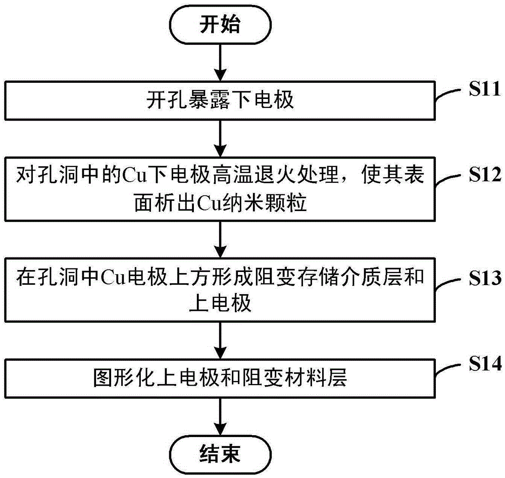
The invention discloses a preparation method of a resistor type memory; the method comprises the following steps: carrying out high temperature annealing to an exposed lower electrode with an opening so as to precipitate nanometer particles on the surface of the electrode; forming a resistance change storage medium layer and an upper electrode above the lower electrode in a hole; schematizing the upper electrode and a resistance change material layer. The preparation method of the resistor type memory is provided; synapse particles are formed on the surface of the electrode under Cu, because local electric field enhancement effect is presented, when resistance changes in the storage medium, a conductive path can be formed in priority above the synapse particles, thereby effectively eliminating activation voltage of an element, improving element yield, and reducing discreteness of element parameters. The CuxO base resistor type memory prepared by the method is low in making cost, good in effect, and can be easily integrated with CMOS technology.

Description

technical field [0001] The invention belongs to the technical field of integrated circuit manufacturing, and in particular relates to a preparation method of a resistance memory which improves the uniformity of device parameters. Background technique [0002] Due to the increasing popularity of portable electronic devices, non-volatile memory has an increasing share in the overall memory market. The current FLASH technology is the mainstream of the non-volatile memory market, accounting for 90% of the market share. However, with the advancement of semiconductor process nodes, FLASH technology is encountering a series of bottleneck problems, such as the floating gate cannot be thinned without limit with the development of technology generations, data retention characteristics, etc. It is reported that the limit of FLASH technology is around 16nm, This forces people to search for a next-generation non-volatile memory with superior performance. Recently, resistive switching m...

Claims


Application Information

Patent Timeline
Patent Type & Authority Patents(China)
IPC IPC(8): H01L45/00
Inventor 吕杭炳刘明刘琦李颖弢龙世兵
Owner INST OF MICROELECTRONICS CHINESE ACAD OF SCI
Learn More