

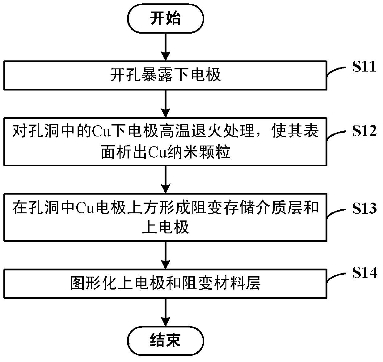
Preparation method of resistor type memory
A resistive and memory technology, which is applied in the direction of electrical components, can solve the problems of floating gates that cannot be thinned and data retention characteristics, and achieve the effects of low manufacturing cost, reduced discreteness, and eliminated activation voltage
- Summary
- Abstract
- Description
- Claims
- Application Information
AI Technical Summary
Problems solved by technology
Method used
Image

Examples
Embodiment Construction
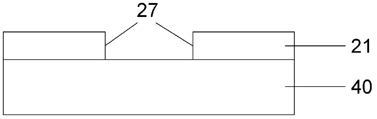
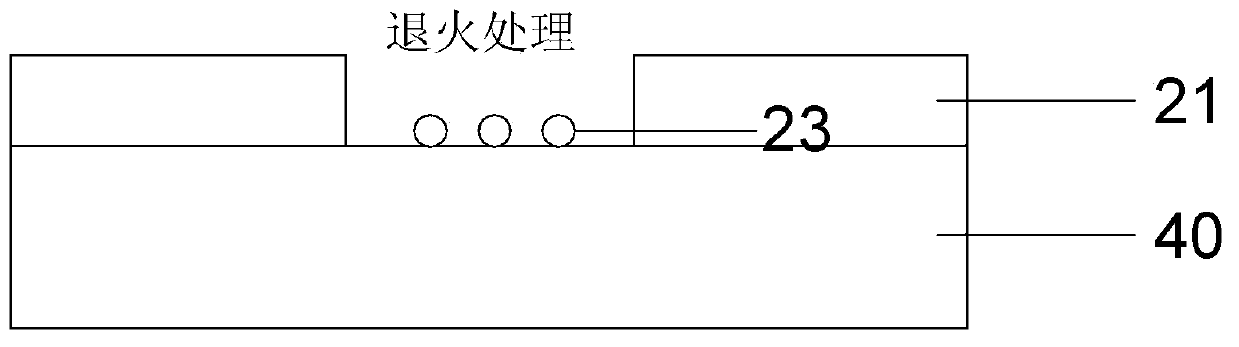
[0023] The present invention provides preferred embodiments, but should not be construed as limited to the embodiments set forth herein. In the drawings, the thicknesses of layers and regions are exaggerated for clarity, but as schematic diagrams, they should not be considered as strictly reflecting the proportional relationship of geometric dimensions.
[0024] The drawings referenced herein are schematic illustrations of idealized embodiments of the invention, and the illustrated embodiments of the invention should not be considered limited to the particular shapes of the regions shown in the drawings, but include resulting shapes, such as manufacturing-induced deviation. For example, the curves obtained by dry etching usually have curved or rounded characteristics, but in the illustrations of the embodiments of the present invention, they are all represented by rectangles, and the representations in the figures are schematic, but this should not be considered as limiting th...
PUM
| Property | Measurement | Unit |
|---|---|---|
| thickness | aaaaa | aaaaa |
| thickness | aaaaa | aaaaa |
Abstract
Description
Claims
Application Information