Method for manufacturing resistive type memory

A resistive and memory technology, applied in the manufacture of semiconductor/solid-state devices, circuits, electrical components, etc., can solve the problems of voids, difficult to effectively control the distribution of O elements, and poor uniformity of the film, so as to eliminate the activation voltage and reduce the production cost. Low, the effect of improving the device yield

Active Publication Date: 2011-11-23
江苏畅微电子科技有限公司
View PDF6 Cites 4 Cited by
  • Summary
  • Abstract
  • Description
  • Claims
  • Application Information

AI Technical Summary

Problems solved by technology

Cu prepared by this method x O-based resistive memory is low in cost and easy to integrate with CMOS technology, but has the following disadvantages: (1) It is easy to integrate on Cu x Voids between O storage medium and Cu matrix
(2) Since the Cu interconnection is generally a polycrystalline structure, when it is oxidized by plasma oxidation or thermal oxidation, the oxidation rate of the grains and grain boundaries is different, resulting in the formation of Cu interconnects. x O film uniformity is poor
(3)Cu x The distribution of O element in the O film is directly related to the performance of the device. It is difficult to effectively control the distribution of O element in the film by plasma oxidation or thermal oxidation.

Method used


Image

  • Method for manufacturing resistive type memory
  • Method for manufacturing resistive type memory
  • Method for manufacturing resistive type memory

Examples


Embodiment Construction

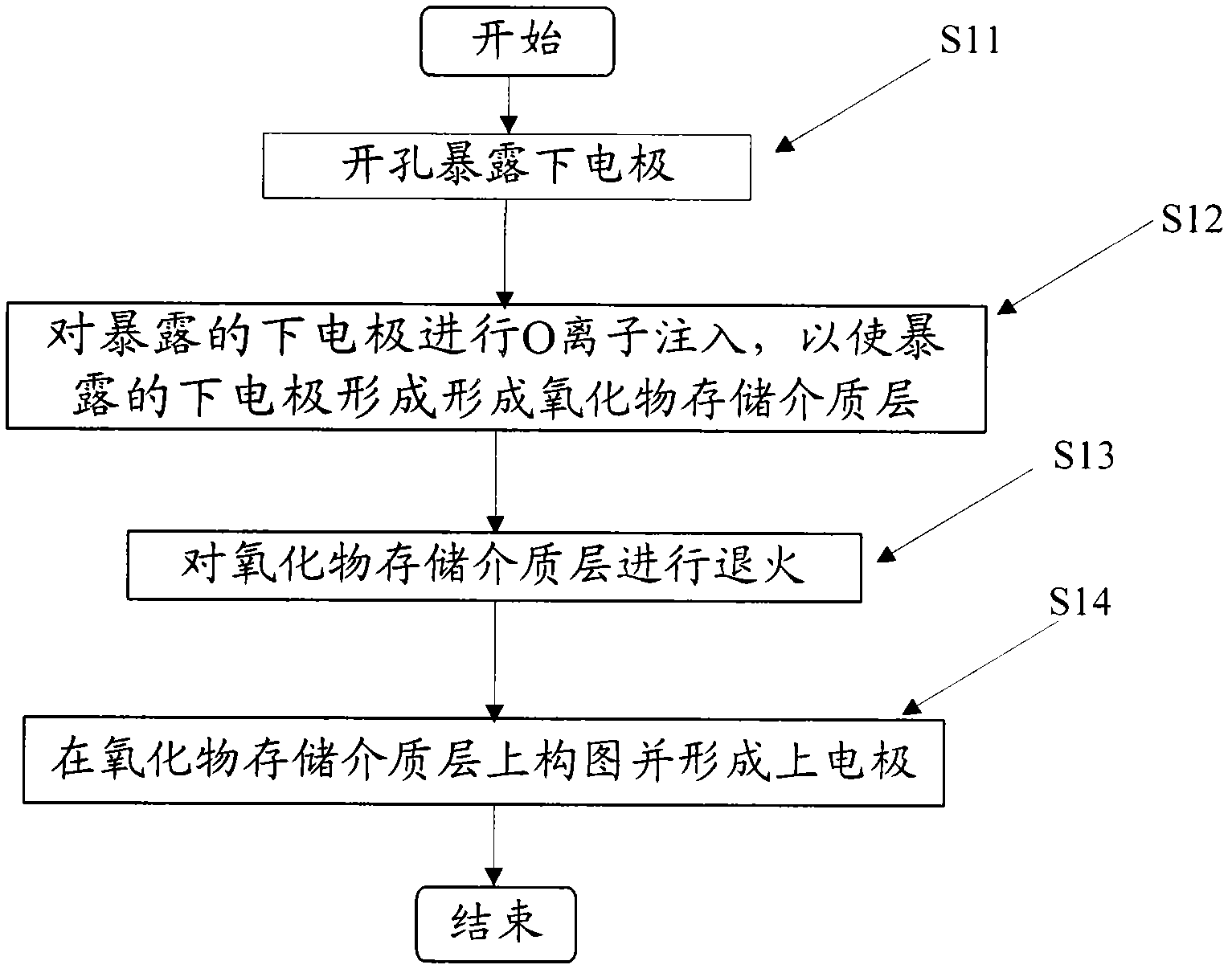
[0042] Hereinafter, the method for preparing the resistance type memory according to the present invention will be described with reference to the accompanying drawings.

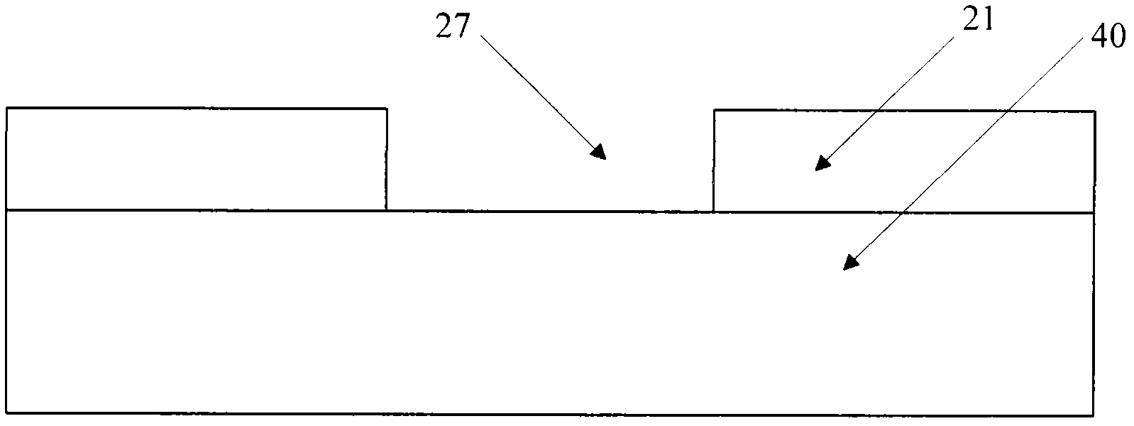
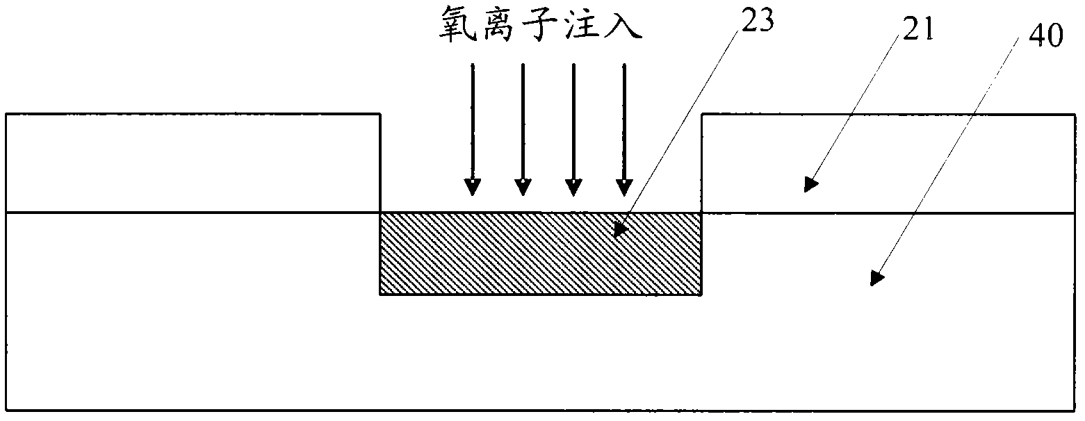
[0043] figure 1 Is a flow chart of the method for manufacturing a resistive memory according to the present invention, Figure 2 to Figure 4 It is a schematic structural decomposition diagram of the manufacturing method of the resistive memory according to the present invention. The following combination Figure 1 to Figure 4 The manufacturing method of the resistive memory is described in detail.

[0044] Reference figure 1 And combine Figure 2 to Figure 4 , The manufacturing method of the resistive memory according to the present invention includes: step S11, opening a hole to expose the bottom electrode, figure 1 with figure 2 As shown; Step S12, O ion implantation is performed on the exposed bottom electrode, so that the exposed bottom electrode forms an oxide storage medium layer, such as figure 1 with ima...


PUM

PropertyMeasurementUnit
thicknessaaaaaaaaaa
thicknessaaaaaaaaaa

Abstract

The invention provides a method for manufacturing a resistive type memory, comprising the following steps: constructing a picture for a lower electrode and carrying out oxygen ion implantation on the lower electrode to form an oxide storage medium layer on the lower electrode; annealing the oxide storage medium layer; and constructing a picture on the oxide storage medium layer and forming an upper electrode. By using the method, an empty hole is not generated between the storage medium layer and the lower electrode; and the oxygen storage medium layer is even, and O elements are distributed evenly in the oxygen storage medium layer. The resistive type memory manufactured by the method has the advantages of low manufacturing cost and good effect and is easy to integrate with a CMOS (complementary metal oxide semiconductor) technology.

Description

Technical field [0001] The invention relates to a method for manufacturing a semiconductor device, and more particularly to a method for manufacturing a resistive memory. Background technique [0002] Memory occupies an important position in the semiconductor market. Due to the continuous popularization of portable electronic devices, non-volatile memories have become more and more important in the overall memory market, and more than 90% of them are occupied by flash memories. However, due to the requirement of stored charge, the floating gate of flash memory cannot be thinned unlimitedly with the development of technology. Reports predict that the limit of flash memory technology is around 32nm, which forces people to look for the next generation of non-volatile memory with superior performance. Memory. [0003] Recently, Resistive Switching Memory has attracted a lot of attention because of its high density, low cost, and ability to break through the limitations of technology ...

Claims


Application Information

Patent Timeline
Patent Type & Authority Applications(China)
IPC IPC(8): H01L21/265H01L45/00
Inventor 王慰
Owner 江苏畅微电子科技有限公司
Why Eureka
Try Eureka