A novel wave-absorbing function design with material and structure wave-absorbing functions being integrated

A wave function and integrated technology, applied to the parts of the instrument, shielding, instruments, etc., can solve the problem of limited structural size adjustment ability, and achieve the effects of wave absorption bandwidth and efficiency, optimized design, and wide range of structural changes

Inactive Publication Date: 2014-03-19
朱嵘飞
View PDF5 Cites 2 Cited by
  • Summary
  • Abstract
  • Description
  • Claims
  • Application Information

AI Technical Summary

Problems solved by technology

On the one hand, its material properties will be constrained or affected by the periodic structure molding, on the other hand, there is a large waste of space in the periodic structure, and its structural size adjustment ability is relatively limited

Method used


Image

  • A novel wave-absorbing function design with material and structure wave-absorbing functions being integrated
  • A novel wave-absorbing function design with material and structure wave-absorbing functions being integrated

Examples


Embodiment 1

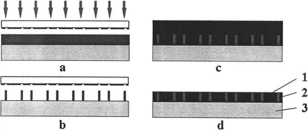
[0019] Such as figure 1 and figure 2 Shown, embodiment 1 comprises the following steps:

[0020] The first step is to mix the SU-8 photoresist and the ferroferric oxide absorbing material at a weight ratio of 10:2, stir well and remove the air bubbles, and then spin-coat it on a glass sheet with a thickness of 1 mm. The spin-coating thickness is 500 Micron.

[0021] The second step is to place the spin-coated glass sheet in an oven for pre-baking to cure the photoresist, the pre-baking temperature is 90 degrees, and the time is 5 hours.

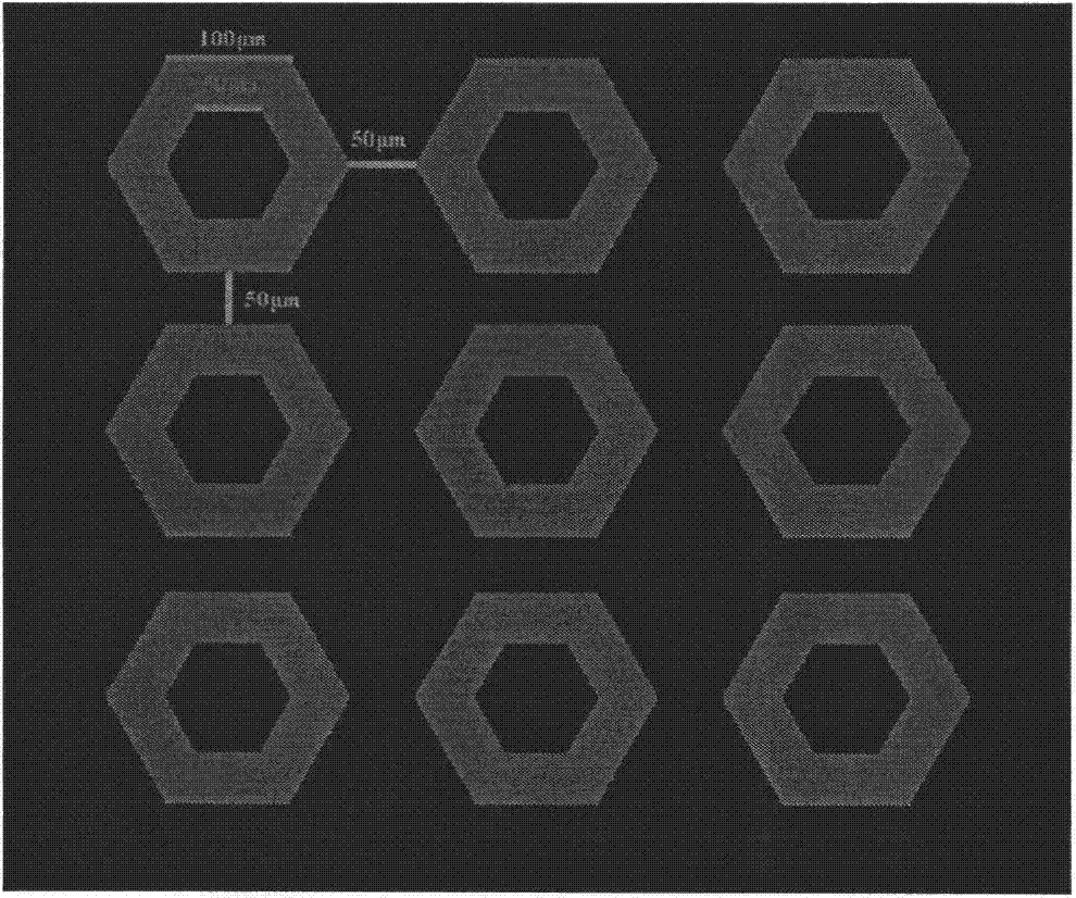
[0022] The third step is to expose the cured photoresist at 10mw / cm 2 Exposure to UV light for 200 seconds. The photoresist structure is a periodic hexagonal honeycomb structure.

[0023] The fourth step, intermediate baking and development, the intermediate drying condition is 90 degrees for one hour, and the developing condition is one hour.

[0024] The fifth step is to fill the metal wave-absorbing material in the hexagonal honeyco...

Embodiment 2

[0027] Such as figure 1 and figure 2 Shown, embodiment 2 comprises the following steps:

[0028] Step 1: Mix SU-8 photoresist and ferroferric oxide absorbing material at a weight ratio of 10:3, stir well and remove air bubbles, then spin-coat on a 1 mm thick glass sheet, the spin-coating thickness is 600 Microns.

[0029] The second step is to place the spin-coated glass sheet in an oven for pre-baking to cure the photoresist. The pre-baking temperature is 90 degrees for 6 hours.

[0030] The third step is to expose the cured photoresist at 10mw / cm 2 Exposure to UV light for 250 seconds. The photoresist structure is a periodic square structure.

[0031] The fourth step, intermediate drying and development, the intermediate drying condition is 90 degrees for 1.5 hours, and the developing condition is 1.2 hours.

[0032] The fifth step is to fill the carbon fiber absorbing material outside the square structure of the photoresist.

[0033] In this embodiment, a dual-mater...

Embodiment 3

[0035] Such as figure 1 and figure 2 Shown, embodiment 2 comprises the following steps:

[0036] Step 1: Mix SU-8 photoresist and ferroferric oxide absorbing material at a weight ratio of 10:3, stir well and remove air bubbles, then spin-coat on a 1 mm thick glass sheet, the spin-coating thickness is 600 Micron.

[0037] The second step is to place the spin-coated glass sheet in an oven for pre-baking to cure the photoresist. The pre-baking temperature is 90 degrees for 6 hours.

[0038] The third step is to expose the cured photoresist at 10mw / cm 2 Exposure to UV light for 250 seconds. The photoresist structure is a periodic cross structure.

[0039] The fourth step, intermediate drying and development, the intermediate drying condition is 90 degrees for 1.5 hours, and the developing condition is 1.2 hours.

[0040] The fifth step is to fill the carbon fiber absorbing material outside the square structure of the photoresist.

[0041] In this embodiment, a dual-materia...


PUM


Abstract

The invention discloses a novel wave-absorbing function design with material and structure wave-absorbing functions being integrated. A thick film characteristic of SU-8 novel negative photoresist is utilized; wave-absorbing materials and the SU-8 photoresist are combined, and micro-electronic technique means is utilized to perform patterning and a periodic structure is formed; and then the area outside the developed photoresist structure is filled with wave-absorbing materials based on wave-absorbing characteristic demands, and thus the wave-absorbing functions of the double materials and double structures are expressed. The thick film characteristic of the SU-8 photoresist is utilized and a patterning method is utilized to give play to the double wave-absorbing function of the materials and the structure; the novel wave-absorbing function design has the technical features of wide structure variable range and large material selection freedom; and the novel wave-absorbing function design facilitates the optimization design of a wave-absorbing system, and helps to improve wave-absorbing bandwidth and efficiency.

Description

technical field [0001] The invention relates to a wave-absorbing function design, in particular to a novel wave-absorbing function design integrating material and structure wave-absorbing functions. Background technique [0002] Absorbing material refers to a class that can absorb and attenuate incident electromagnetic waves, and convert electromagnetic energy into heat energy and dissipate it through the dielectric oscillation, eddy current, and magnetostrictive effects of the absorbent, or make electromagnetic waves disappear due to interference. Functional Materials. People's research on absorbing materials originated from its application in the military field. Today, the development of digital communication has caused a large amount of leakage of electromagnetic waves, making the application range of electromagnetic wave absorbing materials far beyond the military field. Therefore, absorbing materials also have a wide range of needs in television broadcasting, human bod...

Claims


Application Information

Patent Timeline
Patent Type & Authority Applications(China)
IPC IPC(8): G12B17/02
Inventor 朱嵘飞
Owner 朱嵘飞
Why Eureka
Try Eureka