Multi-junction solar cell, photovoltaic conversion component and compound semiconductor layer-by-layer structure

A technology for solar cells and compounds, applied in electrical components, semiconductor devices, energy conversion devices, etc., can solve problems such as lattice mismatch and quality degradation of compound semiconductors

Inactive Publication Date: 2013-04-03
SONY CORP +1
View PDF0 Cites 8 Cited by
  • Summary
  • Abstract
  • Description
  • Claims
  • Application Information

AI Technical Summary

Problems solved by technology

However, in the deformed heterogeneous growth method, there is a problem that the quality of the compound semiconductor is significantly lowered due to the undesired lattice mismatch that is inevitably accompanied.

Method used


Image

  • Multi-junction solar cell, photovoltaic conversion component and compound semiconductor layer-by-layer structure
  • Multi-junction solar cell, photovoltaic conversion component and compound semiconductor layer-by-layer structure
  • Multi-junction solar cell, photovoltaic conversion component and compound semiconductor layer-by-layer structure

Examples


Embodiment 1

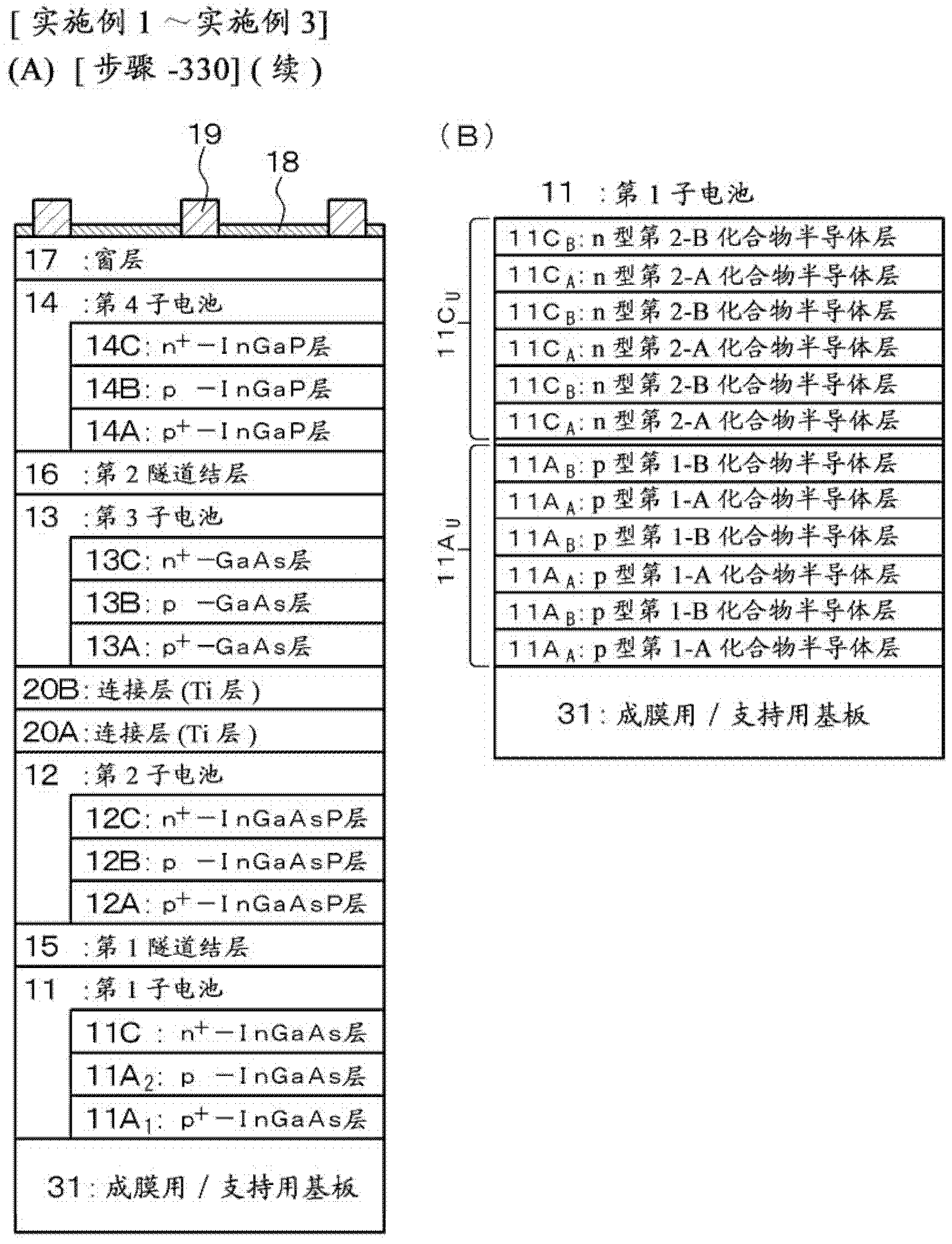
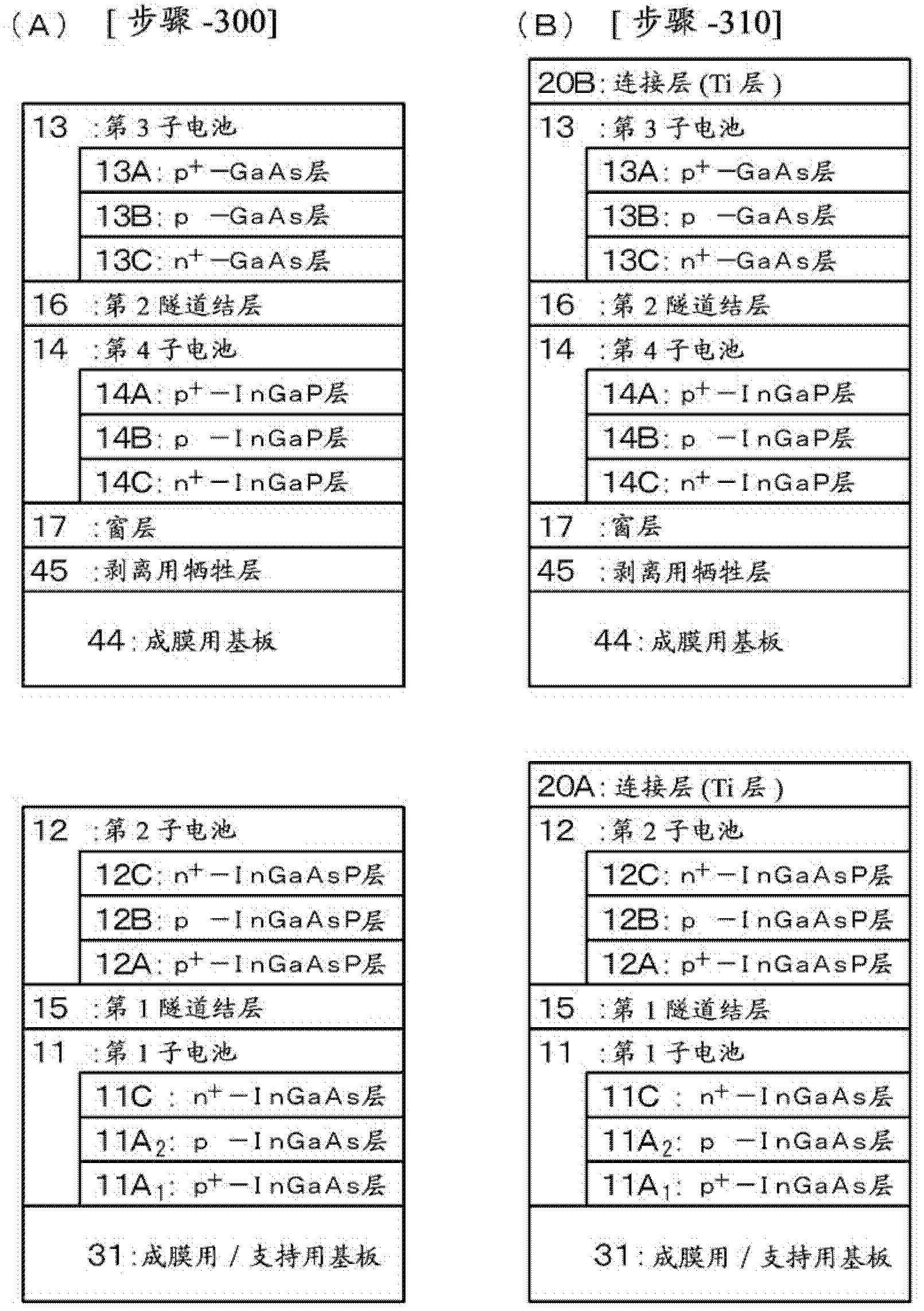
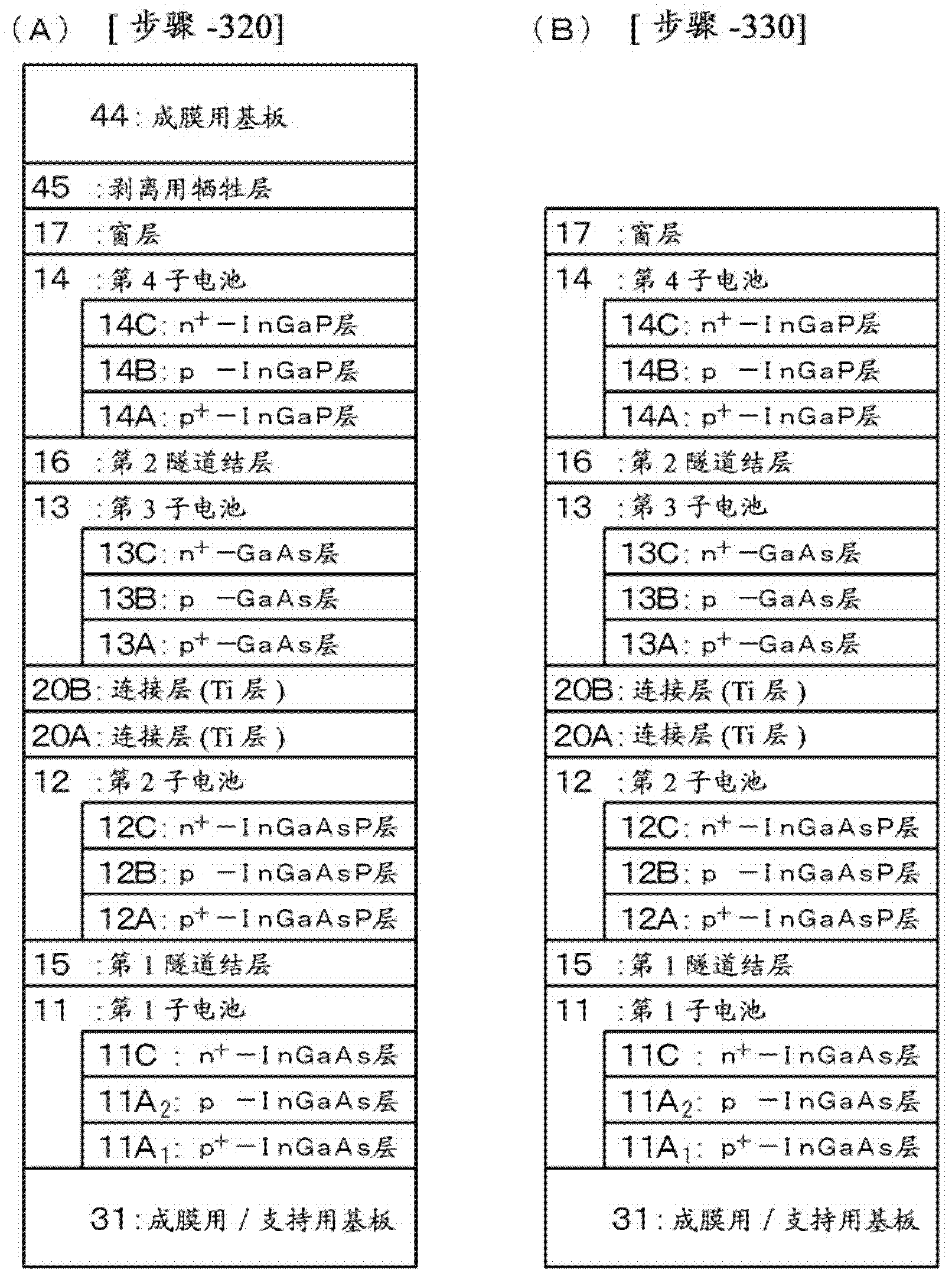
[0112] 2. Example 1 (multi-junction solar cell, photoelectric conversion element, and compound semiconductor layer stacked structure of the present invention)

Embodiment 2

[0113] 3. Embodiment 2 (variation of embodiment 1)

[0114] 4. Embodiment 3 (other modifications of Embodiment 1)

[0115] 5. Embodiment 4 (variation of embodiment 3)

[0116] 6. Embodiment 5 (other modifications of Embodiment 3)

Embodiment 6

[0117] 7. Embodiment 6 (further other modifications of Embodiment 3)

[0118] 8. Embodiment 7 (variation of Embodiment 6), others

[0119] [Comprehensive description of the multi-junction solar cell, photoelectric conversion element, and compound semiconductor layered structure of the present invention]

[0120] In the multi-junction solar cell of the present invention, the specific sub-cell may be located in the lowest layer. The stacking order of the plurality of sub-cells is as follows: the closer to the light incident side, the larger the band gap of the compound semiconductor constituting the sub-cells, that is, from a support substrate, etc. to be described later. From the side to the second electrode side, the band gap increases sequentially. As the case may be, a portion of the plurality of subcells may consist of a Ge layer.

[0121] For the multi-junction solar cell of the present invention, the photoelectric conversion element of the present invention, or the com...


PUM


Abstract

The invention relates to a multi-junction solar cell, a photovoltaic conversion component and a compound semiconductor layer-by-layer structure. The invention provides a multi-junction solar cell with sub-cells, and a sub-cell substrate is matched with a lattice and provided with an expected band gap. The multi-junction solar cell disclosed by the invention is composed of a plurality of sub-cells (11), (12) (13) and (14) which are laminated, each sub-cell is composed of a first compound semiconductor layer and a second compound semiconductor layer which are laminated, at least a special sub-cell (11) is composed of a first layer (11A1, 11A2) and a second layer (11C), the first layer (11A1, 11A2) is composed of a 1-A(th) layer (11AA) and a 1-B(th) layer (11AB) which are laminated, the second layer (11C) is composed of a 2-A(th) layer (11CA) and a 2-B(th) layer (11CB) which are laminated, a combination-A of the 1-A(th) layer (11AA) and the 2-A(th) layer (11CA) is determined based on a band gap value of a specific sub-cell 11, a combination-B of the 1-B(th) layer (11AB) and the 2-B(th) layer (11CB) is determined based on the difference between the lattice constant of the substrate and the lattice constant of the combination-A, and the thicknesses of the 1-B(th) layer (11AB) and the 2-B(th) layer (11CB) are determined based on the difference between the lattice constant of the substrate and the lattice constant of the combination-B, the thickness of the 1-A(th) layer (11AA) and the 2-A(th) layer (11CA).

Description

technical field [0001] The present invention relates to a multi-junction (also referred to as tandem type, stacked type, stacked type) solar cell, a photoelectric conversion element, and a compound semiconductor layer stacked structure using compound semiconductors. Background technique [0002] There are many types of compound semiconductors composed of two or more elements depending on the combination of elements. Furthermore, compound semiconductor devices having various functions and physical properties can be realized by laminating a plurality of compound semiconductor layers made of different materials, and one example thereof is a solar cell. Here, as the solar cell, a silicon-based solar cell using silicon as a semiconductor, a compound semiconductor solar cell using a compound semiconductor, an organic solar cell using an organic material, etc., among them, the compound semiconductor solar cell is being developed in the Development is carried out with the aim of fu...

Claims


Application Information

Patent Timeline
Patent Type & Authority Applications(China)
IPC IPC(8): H01L27/142H01L31/06H01L31/0352H01L31/036
CPCH01L31/0687H01L31/03046H01L31/0352H01L31/06875Y02E10/544
Inventor 吉田浩池田昌夫内田史朗丹下贵志仓本大有持佑之杨辉陆书龙郑新和
Owner SONY CORP
Why Eureka
Try Eureka