
Method for improving data resolution ratio of silica-based optical matrix processor and processor

A processor and resolution technology, applied in the field of optical information processing and optical computing, can solve problems such as difficult to support high-dimensional and high-precision vector-matrix multiplication operations, achieve the number of optical paths and calculation accuracy, increase the number of dimensions, and break through The effect of the resolution bottleneck

Inactive Publication Date: 2014-03-26
INST OF SEMICONDUCTORS - CHINESE ACAD OF SCI
View PDF5 Cites 23 Cited by
  • Summary
  • Abstract
  • Description
  • Claims
  • Application Information

AI Technical Summary

Problems solved by technology

With the increase in the number of optical paths of the optical matrix processor and the improvement of the input data resolution, the dynamic range and resolution requirements of the photodetector and the analog-to-digital converter will increase with the multiplication and accumulation process, and the photodetector and analog-to-digital conversion The limited resolution of the processor will be difficult to support high-dimensional and high-precision vector-matrix multiplication operations

Method used


Image

  • Method for improving data resolution ratio of silica-based optical matrix processor and processor
  • Method for improving data resolution ratio of silica-based optical matrix processor and processor
  • Method for improving data resolution ratio of silica-based optical matrix processor and processor

Examples


Embodiment Construction

[0033]In order to make the object, technical solution and advantages of the present invention clearer, the present invention will be further described in detail below in conjunction with specific embodiments and with reference to the accompanying drawings. It should be noted that, in the drawings or descriptions of the specification, similar or identical parts all use the same figure numbers. Implementations not shown or described in the accompanying drawings are forms known to those of ordinary skill in the art. Additionally, while illustrations of parameters including particular values ​​may be provided herein, it should be understood that the parameters need not be exactly equal to the corresponding values, but rather may approximate the corresponding values ​​within acceptable error margins or design constraints. In addition, the directional terms mentioned in the following embodiments, such as "upper", "lower", "front", "rear", "left", "right", etc., are only referring to...


PUM


Abstract

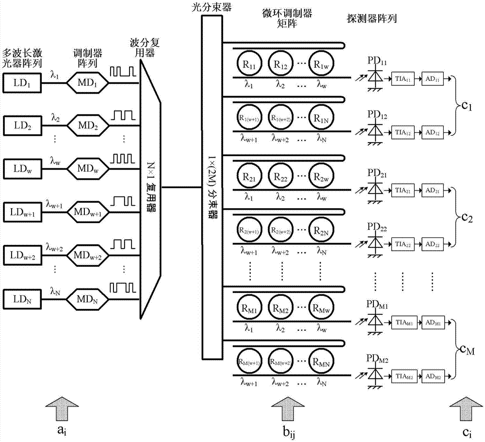
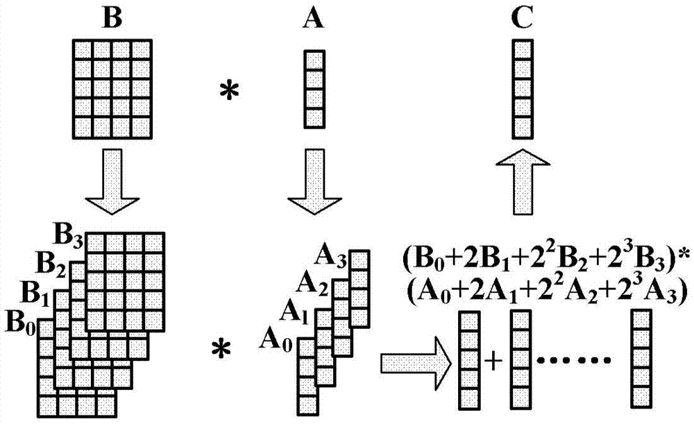
The invention discloses a method for improving the data resolution ratio of a silica-based optical matrix processor and the processor. The method includes the steps that laser signals are output by a laser array and received and modulated by an optical modulator array to an N*1 vector A; a modulator matrix is formed by a micro-ring optical modulator matrix, wherein modulation depths form an M*N matrix B; optical modulation is carried out respectively by dividing the vector A into k subvectors and dividing the matrix B into k submatrixes so as to obtain the product of the k subvectors and the k submatrixes; the obtained product of the subvectors and the k submatrixes is detected by a detector linear array formed by k detectors, and then the product of the vector A and the matrix B is obtained; the element bit wide of each subvector and each submatrix is m, m bit vectors and m bit matrixes are formed after bitwise separation, and the product of the subvectors and the submatrixes is obtained by multiplying the bit vectors by the bit matrixes respectively.

Description

technical field [0001] The invention belongs to the technical field of optical information processing and optical calculation, and in particular relates to a method for improving the data resolution of a silicon-based optical matrix processor and a processor. Background technique [0002] The optical matrix processing technology based on space free optics or planar integrated optics has the characteristics of large bandwidth, strong parallelism, large data throughput, intensive multiplication and accumulation operations, etc., and is very suitable for discrete Fourier transform, linear convolution and loop Matrix-vector multiplication-intensive operations such as convolution, matrix inversion, autocorrelation, and cross-correlation, the basic calculation process is multiply-accumulate. The core operation process of digital signal processing is the multiply-accumulate (MAC) process, so the optical matrix processor and the electrical signal processing module can be integrated ...

Claims


Application Information

Patent Timeline
Patent Type & Authority Applications(China)
IPC IPC(8): G06F17/16
Inventor 周平卢洋洋杨林
Owner INST OF SEMICONDUCTORS - CHINESE ACAD OF SCI
Learn More