Cross-platform multilevel integrated design system for FPGA (field programmable gate array)

An integrated design and FPGA technology, applied in the field of microelectronics, can solve the problems of not providing fast design and verification of FPGA, and achieve the effect of shortening the research and development cycle, improving efficiency, and reducing complex operations

Inactive Publication Date: 2014-03-26
北京微纳星科技有限公司
View PDF6 Cites 32 Cited by
  • Summary
  • Abstract
  • Description
  • Claims
  • Application Information

AI Technical Summary

Problems solved by technology

[0007] In view of this, the main purpose of the present invention is to provide a cross-platform multi-level integrated design system applied to FPGA, to solve the problem that the existing FPGA integrated

Method used


Image

  • Cross-platform multilevel integrated design system for FPGA (field programmable gate array)
  • Cross-platform multilevel integrated design system for FPGA (field programmable gate array)
  • Cross-platform multilevel integrated design system for FPGA (field programmable gate array)

Examples


Embodiment Construction

[0040] In order to make the purpose, technical solution and advantages of the present invention clearer, the present invention will be further described in detail below in conjunction with the accompanying drawings and specific embodiments, so that those skilled in the art can better understand the present invention and implement it, However, the examples given are not intended to limit the present invention. While illustrations of parameters including particular values ​​may be provided herein, it should be understood that parameters need not be exactly equal to the corresponding values, but rather may approximate the values ​​within acceptable error margins or design constraints.

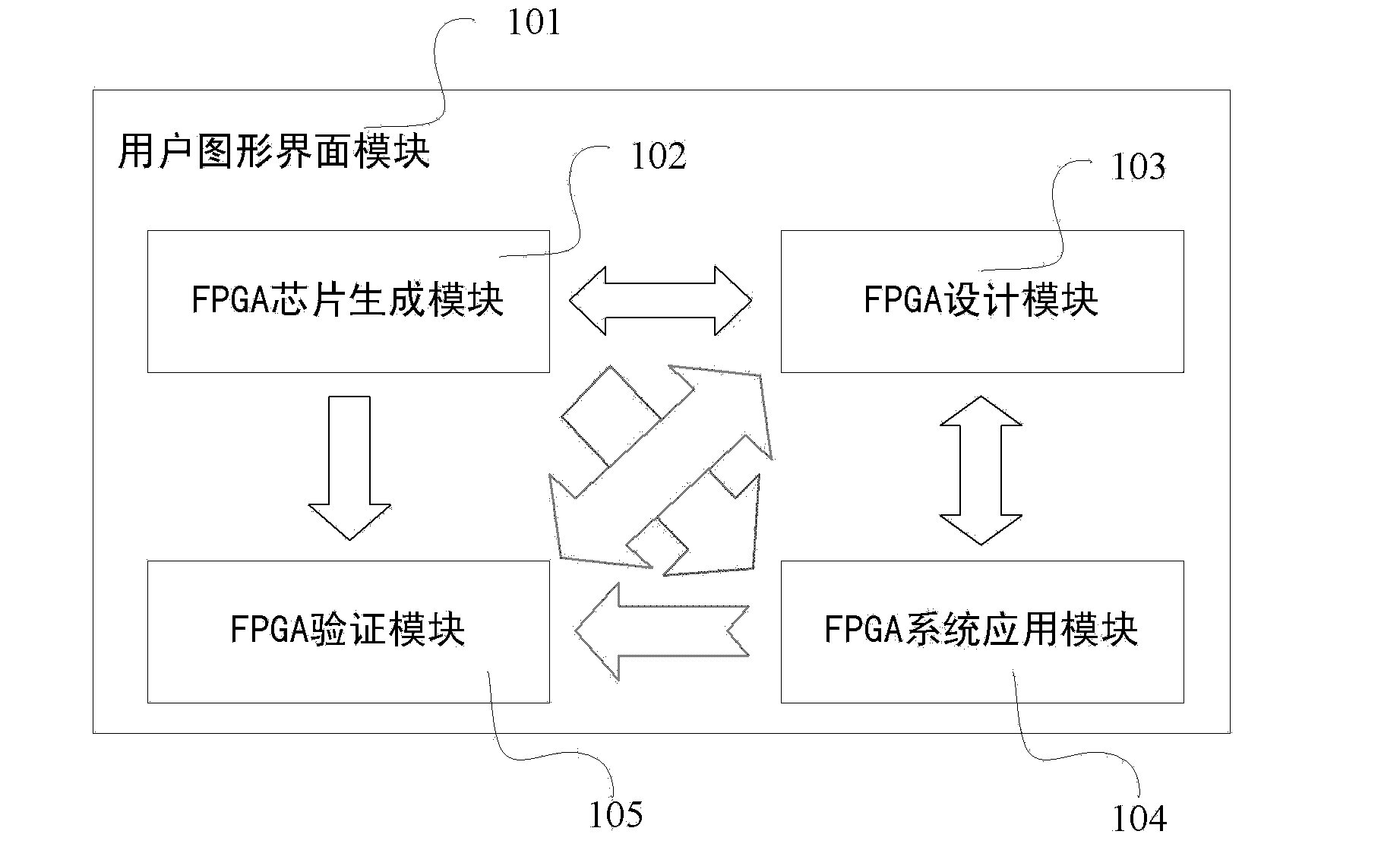
[0041] Such as figure 1 as shown, figure 1 It is a structural block diagram of a multi-level integrated design system for FPGA according to an embodiment of the present invention, and the system includes: graphical user interface module 101, FPGA chip generation module 102, FPGA design module 103...


PUM


Abstract

The invention discloses a cross-platform multilevel integrated design system for an FPGA (field programmable gate array). The cross-platform multilevel integrated design system comprises a user graphical interface module, an FPGA chip generating module, an FPGA design module, an FPGA system application module and an FPGA verification module, wherein the user graphic interface module is used for packaging the FPGA chip generating module, the FPGA design module, the FPGA system application module and the FPGA verification module. Switching among the FPGA chip generating module, the FPGA design module, the FPGA system application module and the FPGA verification module is realized by Tap page switching, so that the FPGA chip generating module, the FPGA design module, the FPGA system application module and the FPGA verification module can be called in a friendly and uniform user graphic interface, and cross-platform operating of Windows, Linux, Mac OS systems can be realized.

Description

technical field [0001] The invention relates to the technical field of integrated circuit design and electronic design automation in the field of microelectronics, in particular to a cross-platform multi-level integrated design system applied to field programmable gate array (Field Programmable Gate Array, FPGA). Background technique [0002] The application and widespread popularity of FPGAs have brought great flexibility to the design of digital systems. FPGA can reconfigure the hardware structure and working mode through software programming, so that hardware design can be as convenient and fast as software design. This has greatly changed the traditional digital system design method, design process and design concept. With the progress of the new generation of FPGA chip technology and design methods and the changes in new application fields and market demands, Electronic Design Automation (EDA) technology has also developed by leaps and bounds. The general trend can be ...

Claims


Application Information

Patent Timeline
IPC IPC(8): G06F17/50
Inventor 张峰于芳李艳韩小炜李明张倩莉陈亮吴利华张国全刘贵宅郭旭峰杨波赵岩王剑李建忠刘忠立陈陵都
Owner 北京微纳星科技有限公司
Why Eureka
Try Eureka