Machining method for high-yield monocrystalline silicon wafer for IGBT

A processing method and technology of silicon wafers, which are applied in the fields of electrical components, semiconductor/solid-state device manufacturing, circuits, etc., can solve the problems of low wafer yield, large amount of polished wafer removal, and long polishing time, etc., so as to increase production capacity, The effect of reducing the amount of polishing removal and shortening the processing time

Active Publication Date: 2014-03-26
ZHONGHUAN ADVANCED SEMICON MATERIALS CO LTD +1
View PDF3 Cites 10 Cited by
  • Summary
  • Abstract
  • Description
  • Claims
  • Application Information

AI Technical Summary

Problems solved by technology

[0005] The purpose of the present invention is to improve the existing processing flow and processing method of the polishing sheet by reducing the depth of the damaged layer of the raw polishing sheet in order to solve the problems of large

Method used


Image

  • Machining method for high-yield monocrystalline silicon wafer for IGBT
  • Machining method for high-yield monocrystalline silicon wafer for IGBT
  • Machining method for high-yield monocrystalline silicon wafer for IGBT

Examples


Embodiment

[0020] This embodiment is a detailed description of the processing flow of a 6-inch 625 μm thick heavily doped sheet:

[0021] (1) Experimental silicon wafer: 6-inch Czochralski silicon abrasive disc, resistivity: 0.02-0.04Ω.cm, thickness 690±5μm, quantity: 120 pieces.

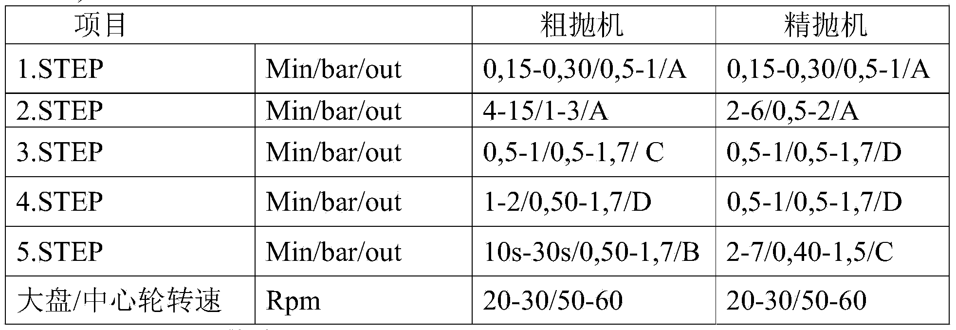
[0022] (2) Processing equipment: acid rot machine, grinding equipment, wax-free polishing machine.

[0023] (3) Auxiliary materials: 325# grinding wheel, 1500# grinding wheel, mixed acid, ceramic plate, rough polishing liquid, fine polishing liquid, template, INSERT (pad for polishing), DIW (deionized water).

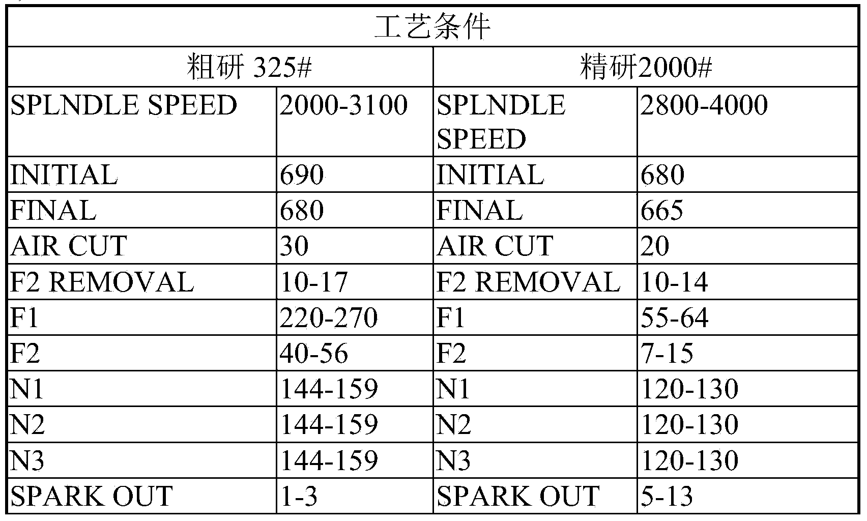
[0024] (4) Method parameter setting:

[0025] a) Grinding:

[0026]

[0027]

[0028] b) Sour rot: mixed acid ratio: HF:HNO 3 :HA C =1:1:2, corrosion time: 40s, washing time: 240s;

[0029] c) Back damage: use Al 2 o 3 , back damage density: ≥5×10⁶ea / cm 2 ;

[0030] d) Back seal: Back seal film thickness: 5000±500A;

[0031] e) Edge removal: processed by automatic edge removal machine, t...


PUM


Abstract

The invention provides a machining method for a high-yield monocrystalline silicon wafer for an IGBT. The method specifically comprises the steps of wafer grinding, grinding, acid corrosion, back damage, back sealing, trimming, polishing, examination and packing and is characterized in that the step of grinding is added between the step of wafer grinding and the step of acid corrosion. The technological process of the whole machining process is adjusted, a wax-free polishing device and a grinding device are matched for production, the damaged layer depth of a raw material grinding wafer is reduced, the polishing removed amount is reduced, and the machining time is shortened on the premise that product quality is ensured, so that productivity of the wax-free polishing process is improved, and earnings are increased.

Description

technical field [0001] The invention relates to a method for producing silicon wafers for insulated gate bipolar transistors (Insulated Gate Bipolar Transistor, referred to as IGBT), in particular to a method for processing high-yield monocrystalline silicon wafers for IGBTs. Background technique [0002] In the process of global informatization and economic globalization, information technology represented by the communication industry, computer industry, network industry, and home appliance industry has achieved rapid development. The application of large-scale integrated circuits, Schottky, metal-oxide - Semiconductor field effect transistors (MOS for short) and other high-power devices are widely used, so the demand for large-scale heavily doped silicon single wafers is increasing year by year. [0003] The main processing flow of large-scale heavily doped silicon single wafer includes: single crystal growth→rolling→slicing→chamfering→grinding→corrosion→back damage→back ...

Claims


Application Information

Patent Timeline
IPC IPC(8): H01L21/304
CPCH01L21/02008H01L21/02013
Inventor 吕莹董建斌曲涛垢建秋李翔
Owner ZHONGHUAN ADVANCED SEMICON MATERIALS CO LTD
Why Eureka
Try Eureka