Method of making a thin film transistor device

A technology of thin film transistors and manufacturing methods, applied in the field of thin film transistors, can solve problems such as increased manufacturing costs, large screen size, and prolonged manufacturing time, and achieve the effects of simplifying manufacturing complexity, shortening manufacturing process time, and reducing costs

Active Publication Date: 2014-03-26
薛英家
View PDF4 Cites 7 Cited by
  • Summary
  • Abstract
  • Description
  • Claims
  • Application Information

AI Technical Summary

Problems solved by technology

Moreover, the screen size of the existing liquid crystal display or organic light-emitting display (OLED) is getting larger and larger. If there are more photomask processes, the relative steps of coating photoresist, exposure, development, and photoresist removal are repeated. The required process cost will increase a lot, and the process time will be relatively longer
Furthermore, the yellow light process between each mask needs to go through a precise alignment process, and the more masks also increase the probability of yellow light misalignment, which leads to the problem of poor yield of the transistors produced

Method used


Image

  • Method of making a thin film transistor device
  • Method of making a thin film transistor device
  • Method of making a thin film transistor device

Examples


Embodiment Construction

[0058] The present invention will be described in detail below in conjunction with the accompanying drawings and embodiments.

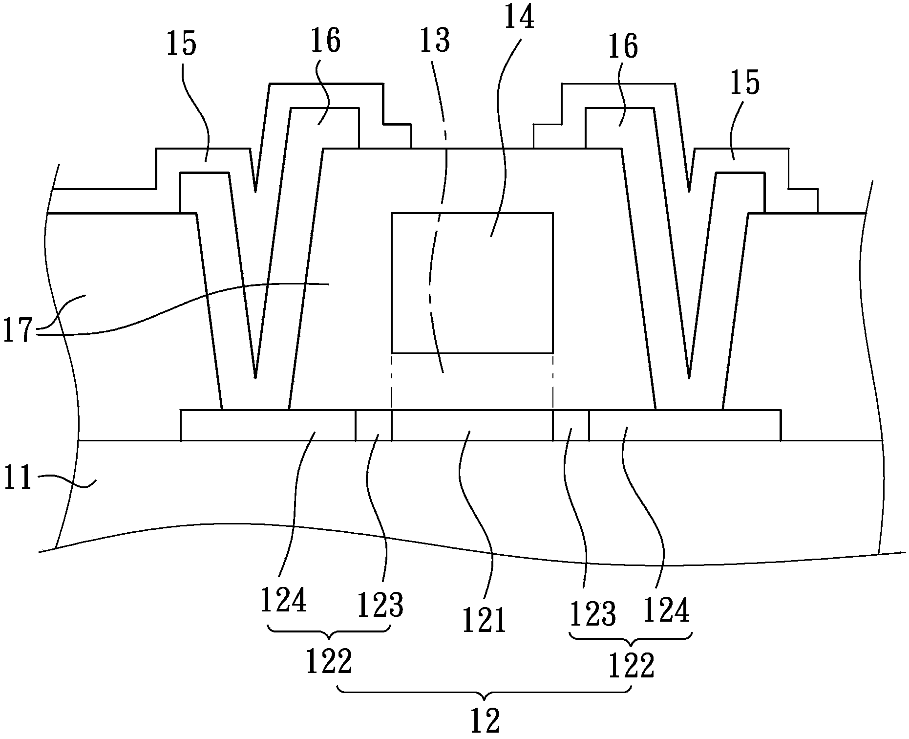
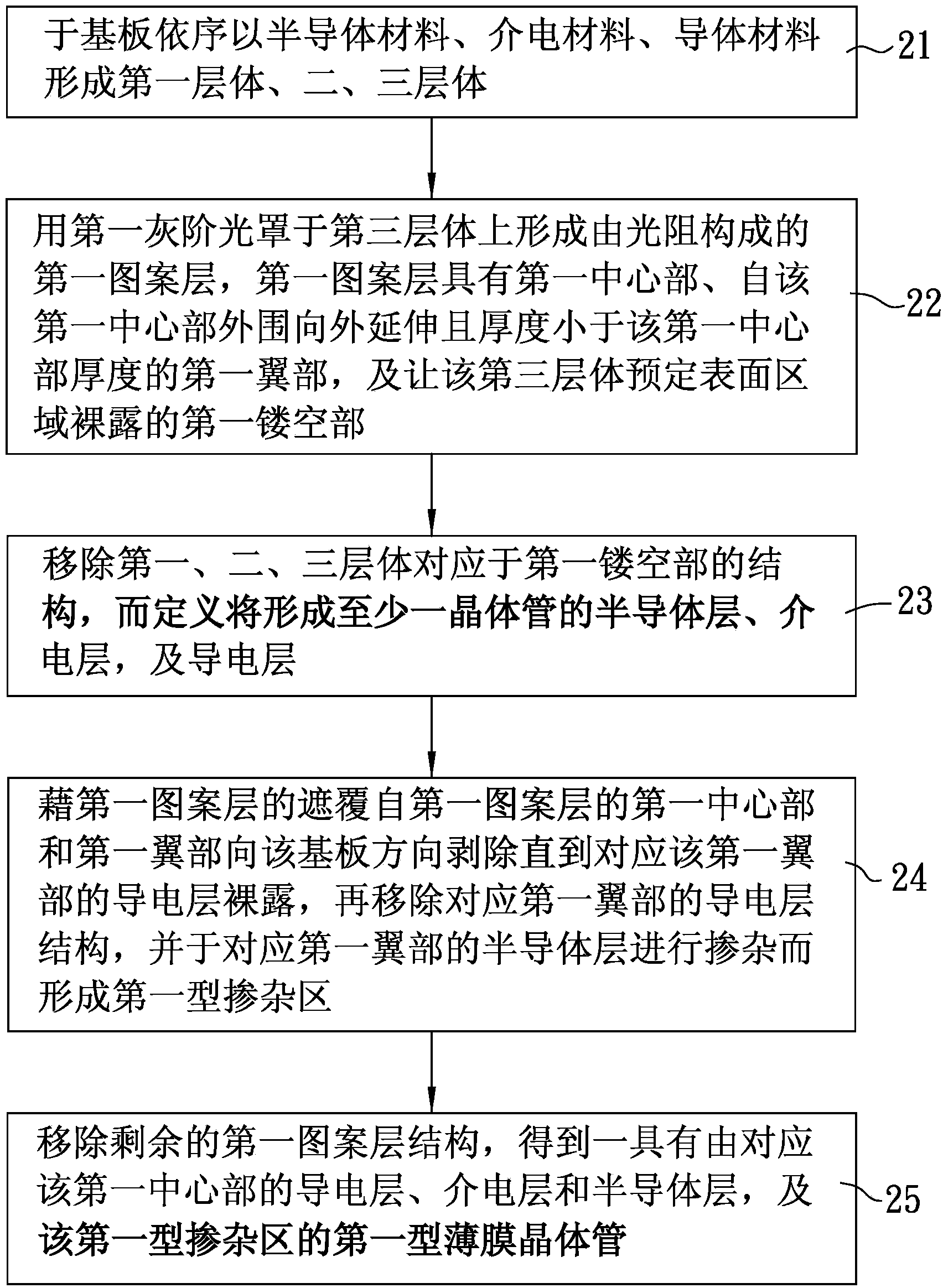
[0059] refer to figure 2 , a first preferred embodiment of the method for fabricating a thin film transistor of the present invention produces at least one first type thin film transistor, and in the following description, the first type thin film transistor is produced to produce such figure 1 The n-type thin film transistor shown is an example, but not limited to n-type thin film transistors, and may also be p-type thin film transistors. The manufacturing method of the n-type thin film transistor includes a step 21 , a step 22 , a step 23 , a step 24 and a step 25 .

[0060] Firstly, the step 21 is performed to form a first layer, a second layer, and a third layer on a substrate sequentially using semiconductor material, dielectric material, and conductive material. Continue, proceed to step 22, use a first gray scale photomask to form a first pa...


PUM


Abstract

The method of making a thin film transistor device includes: forming first pattern layers in different thickness formed by light resistance on a substrate having semiconductor materials, dielectric materials, and conductor materials formed thereon via a first gray-scale mask, gradually removing the first pattern layers, exposing the surfaces of layers from the thinnest part, etching the layers and doping carriers to the semiconductor materials to form a first doping area, and removing the other first pattern layers to obtain a conductive layer, a dielectric layer, and a semiconductor layer corresponding to a first center part and a transistor of the first doping area. The basic frame of a transistor can be made out by means of a gray-scale mask, and compared with a method using multiple masks, the method provided saves more material costs and making time.

Description

technical field [0001] The invention relates to a method for manufacturing a transistor, in particular to a method for manufacturing a thin film transistor. Background technique [0002] In liquid crystal displays, transistors are mainly used in n-type thin film transistors for controlling pixel electrodes, and various n-type thin film transistors, p-type thin film transistors, and complementary transistors in driving circuits for controlling pixel electrodes. In recent years, polysilicon transistors have gradually become one of the mainstream transistors used in displays. [0003] refer to figure 1 , taking the n-type thin film transistor that controls the pixel electrode (not shown) to be electrically connected to it as an example, it mainly includes a substrate 11, an n-type semiconductor layer 12 formed on the substrate 11, and a layer formed on the n-type semiconductor layer. Dielectric layer 13 on the semiconductor layer 12 of type, one layer is arranged on the condu...

Claims


Application Information

Patent Timeline
Patent Type & Authority Applications(China)
IPC IPC(8): H01L21/336H01L21/77
CPCH01L21/32139H01L27/1288H01L21/32133H01L29/66757H01L29/78621
Inventor 薛英家
Owner 薛英家
Why Eureka
Try Eureka