Method for manufacturing three-dimensional flexible stacked encapsulating structure of embedded ultrathin chip

An ultra-thin chip, three-dimensional flexible technology, used in semiconductor/solid-state device manufacturing, semiconductor devices, electrical components, etc., to solve the problem of holding and alignment

Active Publication Date: 2014-03-26
NAT CENT FOR ADVANCED PACKAGING
View PDF5 Cites 10 Cited by
  • Summary
  • Abstract
  • Description
  • Claims
  • Application Information

AI Technical Summary

Problems solved by technology

In addition, this three-dimensional flexible packaging method does not need to hold the thin chip, which effectively solves the problem of holding and aligning the thin chip

Method used


Image

  • Method for manufacturing three-dimensional flexible stacked encapsulating structure of embedded ultrathin chip
  • Method for manufacturing three-dimensional flexible stacked encapsulating structure of embedded ultrathin chip
  • Method for manufacturing three-dimensional flexible stacked encapsulating structure of embedded ultrathin chip

Examples


Embodiment Construction

[0057] In order to make the object, technical solution and advantages of the present invention clearer, the present invention will be described in further detail below in conjunction with specific embodiments and with reference to the accompanying drawings.

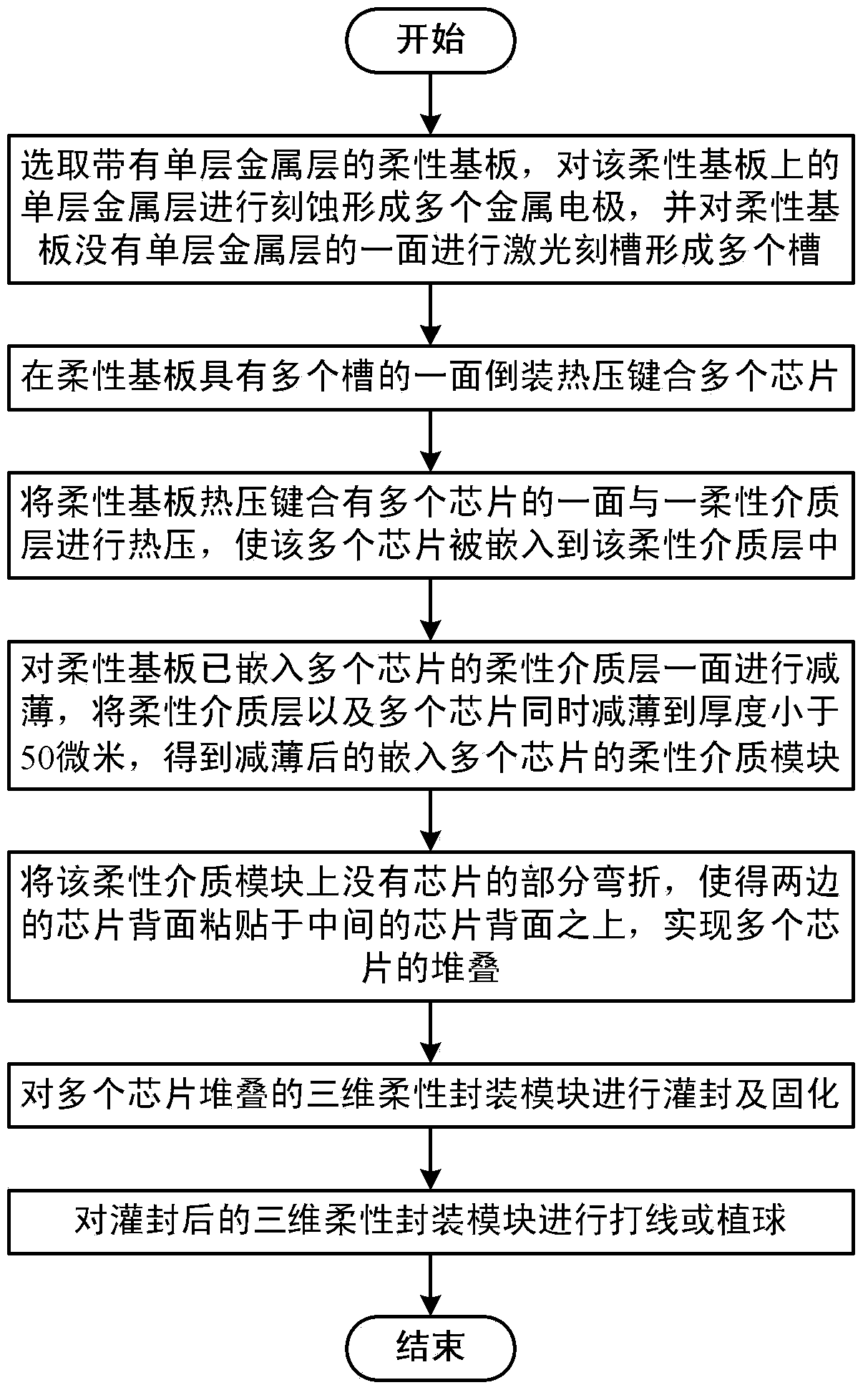
[0058] Such as figure 1 as shown, figure 1 It is a flowchart of a method for manufacturing a three-dimensional flexible package-on-package structure according to an embodiment of the present invention, and the method includes the following steps:

[0059] Step 1: Select a flexible substrate with a single-layer metal layer, etch the single-layer metal layer on the flexible substrate to form multiple metal electrodes, and perform laser grooving on the side of the flexible substrate without a single-layer metal layer to form multiple electrodes. grooves; wherein, the size of the plurality of grooves is consistent with the size of a plurality of metal electrodes formed by etching the single-layer metal layer on the flexible ...


PUM


Abstract

The invention discloses a method for manufacturing a three-dimensional flexible stacked encapsulating structure of an embedded ultrathin chip. The method comprises choosing a flexible substrate with a single-layer metal layer, etching the single-layer metal layer on the flexible substrate to form a plurality of metal electrodes, conducting laser grooving on one side of the flexible substrate without the single-layer metal layer to form a plurality of grooves, conducting flipped thermocompression bonding with a plurality of chips on one side of the flexible substrate, provided with the plurality of grooves, thermally compressing the side of the flexible substrate, provided with the plurality of chips through thermocompression bonding and a flexible medium layer to embed the plurality of chips into the flexible medium layer, thinning one side of flexible medium layer embedded with the plurality of chips of the flexible substrate to obtain a thinned flexible medium module embedded with the plurality of chips, bending a part of the flexible medium module without the chips to stack the chips, encapsulating and curing a three-dimensional flexible encapsulating module with the plurality of stacked chips, and routing or reballing the encapsulated three-dimensional flexible encapsulating module.

Description

technical field [0001] The invention relates to the technical field of system packaging in the microelectronics industry, in particular to a method for manufacturing a three-dimensional flexible stack packaging structure for embedded ultra-thin chips. Background technique [0002] Modern portable electronic products put forward higher requirements for microelectronic packaging. With the continuous pursuit of lighter, thinner, smaller, high reliability and low power consumption, microelectronic packaging is also moving towards higher density and smaller size. Development of smaller packages. In recent years, three-dimensional packaging technology has attracted widespread attention from all over the world. Developed countries such as the United States, European countries, and Japan have invested heavily in related research and development, and have achieved considerable research results. [0003] Three-dimensional packaging technology refers to the three-dimensional high-dens...

Claims


Application Information

Patent Timeline
Patent Type & Authority Applications(China)
IPC IPC(8): H01L21/768H01L21/60
CPCH01L25/50H01L21/56H01L2224/32145H01L2224/73253
Inventor 张霞于大全张博
Owner NAT CENT FOR ADVANCED PACKAGING
Why Eureka
Try Eureka