Unlock instant, AI-driven research and patent intelligence for your innovation.

Multiple times programmable semiconductor device and manufacturing method thereof

A device manufacturing method and multi-time programming technology, which is applied in semiconductor/solid-state device manufacturing, semiconductor devices, electric solid-state devices, etc., can solve the problems of large device area, low integration density, high cost, etc., and achieve simplified device structure and improved Integration density and the effect of reducing the manufacturing process

Active Publication Date: 2016-12-28
INST OF MICROELECTRONICS CHINESE ACAD OF SCI
View PDF5 Cites 0 Cited by
  • Summary
  • Abstract
  • Description
  • Claims
  • Application Information

AI Technical Summary

Problems solved by technology

However, existing FinFET implementations of E 2 The PROM structure is too complex, the device area is large, the process cost is high, and the integration density is low, so it is difficult to apply to large-scale memory cell array manufacturing.
[0005] All in all, the current multi-time programmable semiconductor devices are complex in structure, high in cost and low in efficiency, and urgently need to be improved

Method used


Image

  • Multiple times programmable semiconductor device and manufacturing method thereof
  • Multiple times programmable semiconductor device and manufacturing method thereof
  • Multiple times programmable semiconductor device and manufacturing method thereof

Examples


Embodiment Construction

[0052] The features and technical effects of the technical solution of the present invention will be described in detail below with reference to the accompanying drawings and in conjunction with schematic embodiments, disclosing a high-density integrated multi-time programmable semiconductor device suitable for FinFET technology and a manufacturing method thereof. It should be pointed out that similar reference numerals represent similar structures, and the terms "first", "second", "upper", "lower" and the like used in this application can be used to modify various device structures or process steps . These modifications do not imply spatial, sequential or hierarchical relationships of the modified device structures or process steps unless otherwise specified.

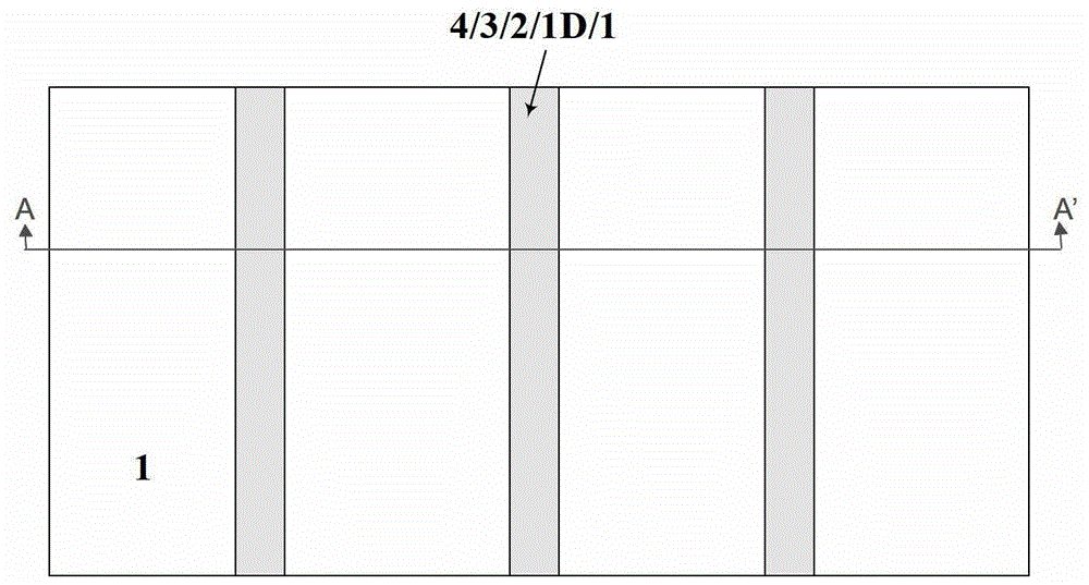
[0053] refer to Figure 6 as well as Figure 1A , Figure 1B , shows a method step S1 according to the present invention, wherein a plurality of fin structures extending along a first direction are formed on a substr...


PUM


Abstract

The invention discloses a multi-time programmable semiconductor device, comprising: a plurality of fin-shaped structures located on a substrate and extending and distributed along a first direction parallel to the surface of the substrate, including a substrate implantation region, a buried oxide layer, and a top layer; a trench The channel region is located in the top layer of the plurality of fin structures; the source and drain regions are located at both ends of the channel region in the top layer of the plurality of fin structures; the gate insulating layer is located on the top and side of the channel region and is parallel to The substrate surface extends in the second direction; the floating gate is located on both sides of the plurality of fin structures in the second direction; the programming / erasing gate is formed by the substrate implantation region and is located under the buried oxide layer. According to the multi-time programmable semiconductor device and its manufacturing method of the present invention, the programming / erasing gate of the FinFET is formed by using the substrate implantation region, which simplifies the device structure, reduces the manufacturing process, and improves the integration density of the device, which is suitable for Multiple times programmable memory.

Description

technical field [0001] The invention relates to a multi-time programmable semiconductor device and a manufacturing method thereof, in particular to a high-density multi-time programmable semiconductor device suitable for Fin Field Effect Transistor (FinFET) technology and a manufacturing method thereof. Background technique [0002] As the feature size of the CMOS process continues to shrink proportionally, the MOS memory structure develops rapidly, and various types of memory cell structures appear. Although DRAM has high integration and low power consumption, it cannot store information for a long time, while SRAM can store information for a long time, but it has a large area and low integration. The current technological development is gradually focusing on ROM, especially electrically erasable E 2 PROM. [0003] Existing E 2 In the PROM cell, the F-N tunneling effect of the thin oxide layer is used to realize electrical erasing, which usually includes an ultra-thin tu...

Claims


Application Information

Patent Timeline
Patent Type & Authority Patents(China)
IPC IPC(8): H01L29/423H01L27/115H01L21/28H01L21/8247H10B69/00
CPCH01L29/42324H01L29/7881H10B41/30H01L29/7855
Inventor 梁擎擎钟汇才朱慧珑
Owner INST OF MICROELECTRONICS CHINESE ACAD OF SCI
Features
  • R&D
  • Intellectual Property
  • Life Sciences
  • Materials
  • Tech Scout
  • Unparalleled Data Quality
  • Higher Quality Content
  • 60% Fewer Hallucinations
Learn More