
Metal-insulating layer-semiconductor back contact interface structure and preparation method for perovskite organic lead halide thin film solar cells

A solar cell and perovskite-type technology, which is applied in the direction of organic semiconductor devices, semiconductor/solid-state device manufacturing, semiconductor devices, etc., can solve the problems of heavy doping difficulties, resistance to high temperature, and resistance to polar solvents, etc., to achieve Back contact, effect of improving efficiency

Active Publication Date: 2017-02-08
深圳市华物光能技术有限公司
View PDF3 Cites 3 Cited by
  • Summary
  • Abstract
  • Description
  • Claims
  • Application Information

AI Technical Summary

Problems solved by technology

However, perovskite-type organic lead halide materials have unstable self-assembled material characteristics such as low temperature resistance and polar solvent resistance, and there is no systematic doping research, which makes heavy doping of them difficult. Difficulties

Method used

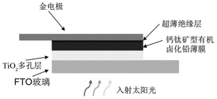
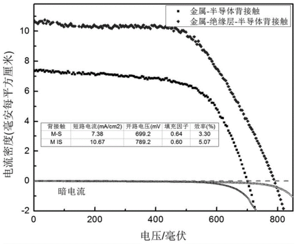
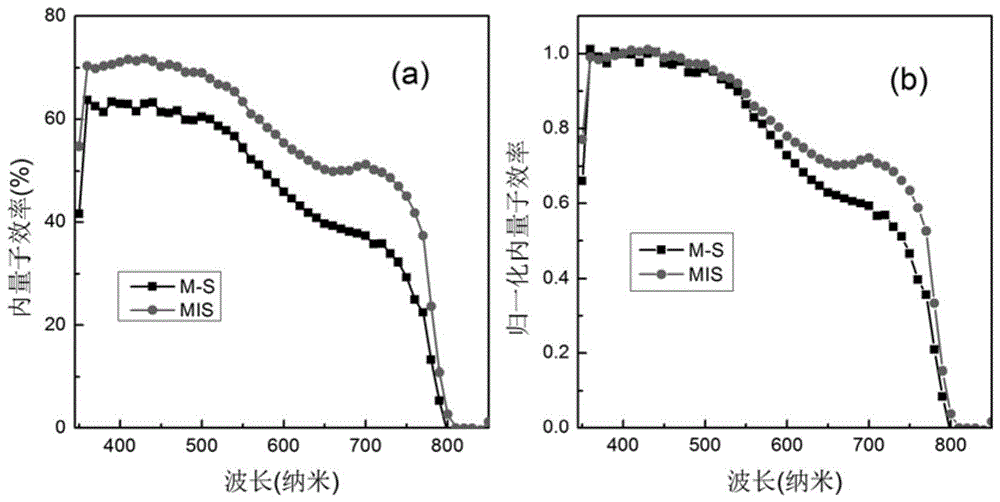

Image

  • Metal-insulating layer-semiconductor back contact interface structure and preparation method for perovskite organic lead halide thin film solar cells
  • Metal-insulating layer-semiconductor back contact interface structure and preparation method for perovskite organic lead halide thin film solar cells
  • Metal-insulating layer-semiconductor back contact interface structure and preparation method for perovskite organic lead halide thin film solar cells

Examples


Embodiment Construction

[0019] The present invention will be further described below in conjunction with the accompanying drawings.

[0020] Figure 5 shows the schematic diagram of the experimental process of atomic layer deposition of ultra-thin oxide insulating layer on the perovskite organic lead halide film.

[0021] Firstly, heat the thin film substrate to a certain temperature (80°C) and vacuum the deposition chamber to a low vacuum, generally controlled at about 1Pa.

[0022] Then, through control, the first step reactant—organometallic precursor (such as trimethylaluminum) is introduced into the cavity for a certain period of time (0.5s), as shown by arrow 1. followed by purge gas N 2 For a certain period of time (5s), the organometallic precursors that failed to adsorb on the surface of the film were taken away, as shown by arrow 3. Then pass the second step reactant H 2 O for a certain period of time (0.5s), as shown by arrow 2, can generate atomic layer metal oxides through the reaction...


PUM


Abstract

The invention discloses a metal-insulating layer-semiconductor back contact interface structure for a perovskite type organic lead halide thin film solar cell and a preparation method thereof. The interface structure is to deposit a layer of uniform oxide insulating layer with controllable thickness on the organic lead halide film by means of atomic layer deposition, which is used to modify and regulate the back contact of the thin film solar cell to achieve the effect of improving the performance of the solar cell. The invention breaks through the traditional back contact structure of the perovskite organic lead halide thin film battery, realizes good back contact without high doping, and improves the photoelectric conversion efficiency of the solar cell. The battery interface structure of the present invention can also be used in other electronic devices that have strict requirements on materials and interfaces.

Description

technical field [0001] The invention relates to the technical field of thin-film solar cells, in particular to a back contact interface structure of a perovskite-type organic lead halide thin-film solar cell and a preparation method thereof. Background technique [0002] Traditional inorganic semiconductor solar cells have problems such as high cost and high pollution, so it is necessary to find new materials that are easy to synthesize, low cost and environmentally friendly for the third generation of thin film solar cells. [0003] Perovskite-type organic lead halide materials (such as CH 3 NH 3 Pb(I,Br,Cl) 3 ) has attracted the attention and research interest of many researchers in recent years due to its excellent photoelectric properties and easy synthesis. Through hard work, the efficiency of thin-film solar cells based on this material and organic hole transport materials has reached 15% internationally, which has great application potential. But at present, the c...

Claims


Application Information

Patent Timeline
Patent Type & Authority Patents(China)
IPC IPC(8): H01L51/52H01L51/56
CPCH10K30/354H10K2102/00Y02E10/549Y02P70/50H10K85/50
Inventor 孟庆波石将建徐余颛罗艳红李冬梅
Owner 深圳市华物光能技术有限公司
Learn More