Ultra-wide band electromagnetic band-gap structure

A technology of electromagnetic bandgap structure and electromagnetic bandgap unit, which is applied in the direction of printed circuit components, etc., can solve problems such as high-frequency synchronous switching noise, etc., and achieve the effect of easy implementation and high efficiency

Inactive Publication Date: 2014-03-26
XIDIAN UNIV
View PDF2 Cites 4 Cited by
  • Summary
  • Abstract
  • Description
  • Claims
  • Application Information

AI Technical Summary

Problems solved by technology

Among them, adding a decoupling capacitor between the power supply and the ground plane is the most commonly used method, but when the frequency is higher than 600MHz, there is a parasitic inductance in the decoupling capacitor, and the parasitic inductance will self-resonate with the capacitor, which lim

Method used


Image

  • Ultra-wide band electromagnetic band-gap structure
  • Ultra-wide band electromagnetic band-gap structure
  • Ultra-wide band electromagnetic band-gap structure

Examples


Embodiment 1

[0022] like figure 1 As shown, an ultra-broadband electromagnetic bandgap structure at least includes a non-conductive substrate 1, the non-conductive substrate 1 is covered with a metal plate 2, and the metal plate 2 is corroded into electromagnetic bandgap units 3 distributed at intervals; Two tape gap units 3 are arranged side by side.

Embodiment 2

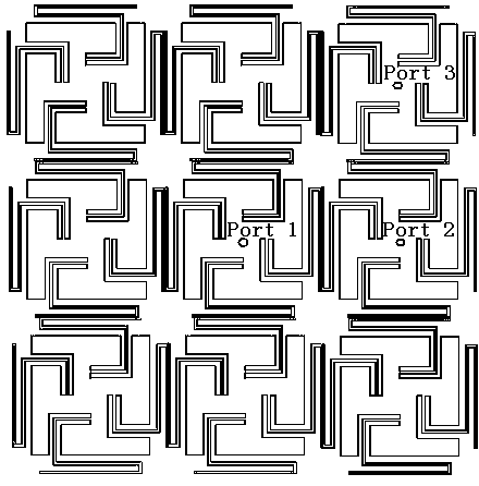
[0024] like figure 2 As shown, an ultra-broadband electromagnetic bandgap structure at least includes a non-conductive substrate 1, the non-conductive substrate 1 is covered with a metal plate 2, and the metal plate 2 is corroded into electromagnetic bandgap units 3 distributed at intervals; There are nine tape gap units 3, and the nine are distributed into a 3*3 square.

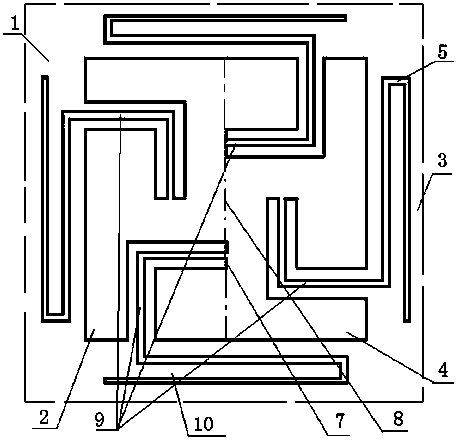
[0025] like image 3 As shown, the electromagnetic bandgap unit 3 is composed of a square body 4 on one side of the non-conductive substrate 1, conductor lines 5 extending outward on the four sides of the square body, and an L-bridged EBG structural unit 6 on the other side, and the four sides are outwardly The extended conductor line 5 is perpendicular to the four sides of the square body 4, and the four sides extend outward. The conductor line 5 extends outward from the 1 / 3-1 / 4 position of the connecting side, and the starting point 7 is close to the vertical center line 8 of the square body, The non-co...


PUM

PropertyMeasurementUnit
Thicknessaaaaaaaaaa

Abstract

The invention is applied to the field of printed circuit boards, and particularly relates to an ultra-wide band electromagnetic band-gap structure applied to power planes of printed circuit boards. The elementary cell of the ultra-wide band electromagnetic band-gap structure consists of spinning branches and slots of square metal patches. The spinning branches of the elementary cell of the electromagnetic band-gap structure surround the square metal patches. The slots are etched on the metal patches of the elementary cell of the electromagnetic band-gap structure. Four sides of the metal patches of the elementary cell of the electromagnetic band-gap structure are grooved. The electromagnetic band-gap structure has wider bandwidth and lower cut-off frequency, basically covers noise band of noises of a synchronous switch, and can eliminate noises of the synchronous switch between the power planes and the ground plane omnidirectionally. The ultra-wide band electromagnetic band-gap structure produced by the conventional printed circuit board manufacturing process is easy to realize and has high benefit.

Description

technical field [0001] The invention is applied to the field of printed circuit boards, and in particular relates to an ultra-wideband electromagnetic bandgap structure applied to the power supply plane of the printed circuit board. Background technique [0002] With the development of modern high-speed digital circuits, the problem of synchronous switching noise between the power plane and the ground plane has become more and more prominent due to reasons such as fast edge rise rate, high clock rate and low voltage level. Synchronous switching noise is caused by multiple resonance modes between the power plane and the ground plane when the currents of multiple active devices on the printed circuit board are switched simultaneously, and synchronous switching noise will cause problems such as signal integrity and electromagnetic compatibility. The printed circuit board is a very important part of the electromagnetic compatibility in the system, so how to eliminate the syn...

Claims


Application Information

Patent Timeline
IPC IPC(8): H05K1/02
Inventor 路宏敏梁博王向荣
Owner XIDIAN UNIV
Why Eureka
Try Eureka