
TN (twisted nematic) type liquid crystal display panel, TN type liquid crystal display panel preparation method and liquid crystal display device

A liquid crystal panel, one-sided technology, applied in the direction of nonlinear optics, instruments, optics, etc., can solve the difficult problem of realizing narrow frame design of TN-type liquid crystal display panel, and achieve the effect of realizing narrow frame design and reducing frame

Active Publication Date: 2014-04-02
HEFEI BOE OPTOELECTRONICS TECH +1
View PDF4 Cites 7 Cited by
  • Summary
  • Abstract
  • Description
  • Claims
  • Application Information

AI Technical Summary

Problems solved by technology

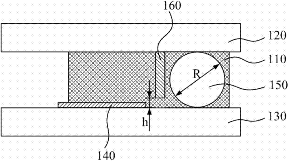
In order to avoid the short circuit of the gate shift register 050 caused by the contact between the gold ball 040 and the gate shift register 050 arranged on the side of the lower substrate 020 facing the upper substrate 010, it is required that the gate shift register 050 and the sealing frame containing the gold ball 040 Adhesive 030 must maintain a certain safety distance. This safe distance must at least be guaranteed to be greater than the coating accuracy of sealant 030 to meet the coating requirements of sealant 030. Therefore, it is difficult to realize the narrow frame design of TN-type LCD panels.

Method used


Image

  • TN (twisted nematic) type liquid crystal display panel, TN type liquid crystal display panel preparation method and liquid crystal display device
  • TN (twisted nematic) type liquid crystal display panel, TN type liquid crystal display panel preparation method and liquid crystal display device
  • TN (twisted nematic) type liquid crystal display panel, TN type liquid crystal display panel preparation method and liquid crystal display device

Examples


Embodiment 1

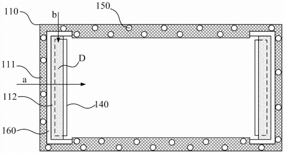
[0038] Please refer to figure 2, the first embodiment provides a TN-type liquid crystal panel, including: an upper substrate 120 and a lower substrate 130 connected to the box through a sealant 110, and the side of the upper substrate 120 facing the lower substrate 130 has a pixel electrode (not shown in the figure out), the side of the lower substrate 130 facing the upper substrate 120 has a common electrode (not shown in the figure) and a gate shift register 140; the sealant 110 includes gold balls 150 doped with conductive pixel electrodes and common electrodes The main sealant 111, and the secondary sealant 112 not doped with gold balls; the side of the upper substrate 120 facing the lower substrate 130 is provided with a retaining wall 160, and the retaining wall 160 is located between the main sealant 111 and the secondary sealant 112 and separates the gate shift register 140 from the primary sealant 111 , the secondary sealant 112 and the gate shift register 140 also h...

Embodiment 2

[0051] On the basis of the TN-type liquid crystal panel provided in the first embodiment above, the second embodiment provides a liquid crystal display device, which has the TN-type liquid crystal panel provided in the first embodiment above.

[0052] In the TN-type liquid crystal panel provided by the above solution, when the coating width of the sealant is constant, along the width direction of the sealant, there will be a certain overlapping area between the secondary sealant and the gate shift register. , so that the frame width of the entire liquid crystal panel can be set smaller, therefore, in the liquid crystal display device provided by the present invention with the above-mentioned TN type liquid crystal panel, the frame of the liquid crystal display device can also be made very small, so as to facilitate the realization of liquid crystal display. Narrow bezel design for display devices.

Embodiment 3

[0054] exist Figure 4 based on the reference Figure 5a ~ Figure 5e , this embodiment also provides a method for preparing the TN-type liquid crystal panel provided in Embodiment 1, including:

[0055] Step 401, such as Figure 5a As shown, the barrier wall 160 is prepared on the pixel electrode of the upper substrate 120; Figure 5b As shown, a gate shift register 140 is prepared on the common electrode of the lower substrate 130;

[0056] Step 402, such as Figure 5c As shown, in the coated area of ​​the upper substrate 120, the part located inside the retaining wall 160 is coated with the secondary sealant 112 of the undoped gold ball 150; Figure 5d As shown, the main sealant 111 doped with gold balls 150 is coated in other parts of the coating area;

[0057] Step 403, such as Figure 5e As shown, the upper substrate 120 and the lower substrate 130 are connected to the box; wherein, after the box is boxed, the barrier wall 160 separates the gate shift register 140 f...


PUM

PropertyMeasurementUnit
Thicknessaaaaaaaaaa

Abstract

The invention discloses a TN type liquid crystal display panel comprising an upper substrate and a lower substrate which are connected in a folded manner through frame sealing adhesives. One surface of the upper substrate facing the lower substrate is provided with pixel electrodes and retaining walls, one surface of the lower substrate facing the upper substrate is provided with common electrodes and gate shifting registers, the frame sealing adhesives include primary frame sealing adhesives and secondary frame sealing adhesives, golden balls conducting the pixel electrodes and the common electrodes are doped in the primary frame sealing adhesives, golden balls are not doped in the secondary frame sealing adhesives, the retaining walls are positioned among the primary frame sealing adhesives and the secondary frame sealing adhesives, the gate shifting registers are separated from the primary frame sealing adhesives, and the secondary frame sealing adhesives and the gate shifting registers have overlapped areas. By the aid of the technical scheme, a narrow frame of the TN type liquid crystal display panel can be designed. In addition, the invention further provides a TN type liquid crystal display panel preparation method and a liquid crystal display device with the TN type liquid crystal display panel.

Description

technical field [0001] The invention relates to the technical field of manufacturing liquid crystal display devices, in particular to a TN type liquid crystal panel, a preparation method thereof, and a liquid crystal display device. Background technique [0002] Thin Film Transistor Liquid Crystal Display (TFT-LCD) has the advantages of small size, low power consumption, and no radiation. It has developed rapidly in recent years and has become the mainstream of displays on the market. With the rapid development of TFT-LCD, the narrow frame structure has become a very important direction in its future development. TFT-LCD is mainly composed of a liquid crystal display panel and a backlight module, and the market demand for a narrow frame is mainly reflected in the peripheral structure of the liquid crystal display panel. [0003] The manufacturing process of the liquid crystal display panel mainly includes: forming a color filter array on the upper substrate, forming a TFT a...

Claims


Application Information

Patent Timeline
IPC IPC(8): G02F1/1339G02F1/1333
Inventor 王炎陈俊生王春
Owner HEFEI BOE OPTOELECTRONICS TECH
Learn More