Gold foil cutting method

A gold foil and cutting technology, applied in the field of thin-film circuit processing and production, can solve the problems of inability to process gold foil for pressure welding, poor edge flatness, etc., and achieve the effect of improving processing efficiency and improving consistency

Inactive Publication Date: 2014-04-09
THE 41ST INST OF CHINA ELECTRONICS TECH GRP
View PDF3 Cites 6 Cited by
  • Summary
  • Abstract
  • Description
  • Claims
  • Application Information

AI Technical Summary

Problems solved by technology

However, the high heat of the laser during the processing will cause the ablation of the edge of the gold foil, making the edge flatness worse, and it cannot meet the needs of gold foil processing for pressure welding.

Method used


Image

  • Gold foil cutting method
  • Gold foil cutting method
  • Gold foil cutting method

Examples


Embodiment 1

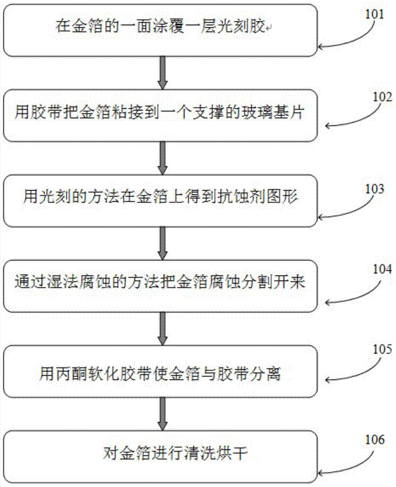
[0031] Such as figure 1 as shown, figure 1 A flow chart of a gold foil cutting method provided by the present invention, the method includes the following steps:

[0032] Step 101: coating a layer of photoresist on one side of the gold foil;

[0033] Step 102: bonding the gold foil to a supporting glass substrate with adhesive tape;

[0034] Step 103: Obtain a resist pattern on the gold foil by photolithography;

[0035] Step 104: Etching and dividing the gold foil by wet etching;

[0036] Step 105: soften the tape with acetone to separate the gold foil from the tape;

[0037] Step 106: Washing and drying the gold foil.

[0038] In the step 101, the gold foil used is pure gold with a purity of 99.99%, the thickness of the gold foil is 0.02mm, and the size is 40mm×40mm;

[0039] In the step 101, a layer of photoresist is coated on one side of the gold foil using a coater;

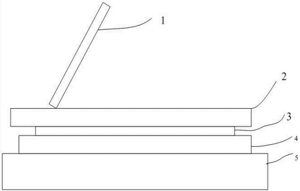
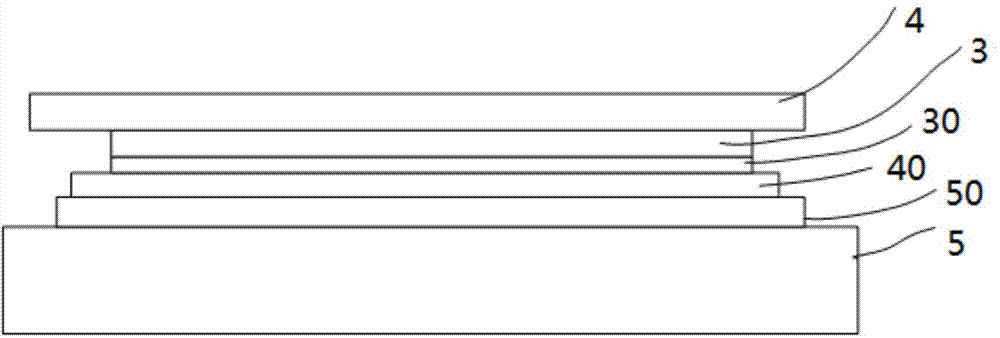
[0040] In the step 101, the UV tape 4 is used to bond the gold foil 3 before gluing, then the UV t...

Embodiment 2

[0058] On the basis of the foregoing embodiments, further, as Figure 1-Figure 5 Shown, a kind of gold foil cutting method, wherein, comprises the following steps:

[0059] Step 101: Coating a layer of photoresist on one side of the gold foil; Step 102: Bonding the gold foil to a supporting glass substrate with an adhesive tape; Step 103: Obtaining a resist pattern on the gold foil by photolithography; Step 104: etching the gold foil into predetermined sizes and shapes by wet etching; step 105: softening the tape with acetone to separate the gold foil from the tape; step 106: cleaning and drying the gold foil.

[0060] In the step 101, the gold foil is pure gold with a purity of 99.99%, the thickness of the gold foil is 0.02mm, and the size is 40mm×40mm; The method is to use UV tape to bond the gold foil before gluing, then put the UV tape with gold foil on a flat glass substrate, then cover the gold foil with a layer of plastic film, and use a flat scraper to scrape the gold...


PUM

PropertyMeasurementUnit
thicknessaaaaaaaaaa
thicknessaaaaaaaaaa
thicknessaaaaaaaaaa

Abstract

The invention provides a gold foil cutting method which comprises the following steps: coating one side of a gold foil with a layer of photoresist, using an adhesive tape to adhere the gold foil to a supporting glass substrate, using a photo-etching method to obtain a resist pattern on the gold foil, segmenting gold foil etch through a wet etching method, softening the adhesive tape with the use of acetone to separate the gold foil from the adhesive tape, and cleaning and drying the gold foil to obtain the needed gold foil dimension. The problem that the gold foil is difficult to clamp in the photo-etching process is solved by adding the glass substrate support, and the consistency and dimension processing precision of gold foil cutting are ensured by the use of the photo-etching method. Compared with a manual cutting method, the processing efficiency is greatly improved, and the gold foil cutting method is suitable for mass production and is worthy to be popularized in production.

Description

technical field [0001] The invention belongs to the field of film circuit processing and manufacture, and in particular relates to a gold foil cutting method. Background technique [0002] Broadband coaxial attenuator is a commonly used microwave device, which is applied in many instruments and systems. The cavity structure of the suspension line is usually adopted, and the ceramic film attenuator is welded into the cavity by soldering. The ceramic attenuation piece is connected with the elastic bellows through side metallization. The metallization of the side of the ceramic attenuator is usually realized by hot-press welding with gold foil ring wrapping. The quality of gold foil processing will have a great impact on the quality of the gold foil bonding of the attenuator and the performance indicators of the attenuator. Therefore, the gold foil used for bonding has strict requirements on its dimensional tolerance and flatness. [0003] The thickness of gold foil used for...

Claims


Application Information

Patent Timeline
Patent Type & Authority Applications(China)
IPC IPC(8): H05K3/06
Inventor 王进刘金现马子腾
Owner THE 41ST INST OF CHINA ELECTRONICS TECH GRP
Why Eureka
Try Eureka