Manufacturing method of copper-copper bonding salient points

A technology of copper-copper bonding and manufacturing method, which is applied in the direction of semiconductor/solid-state device manufacturing, electrical components, electrical solid-state devices, etc. Surface flatness requirements, etc.

Active Publication Date: 2014-04-16
NAT CENT FOR ADVANCED PACKAGING
View PDF8 Cites 11 Cited by
  • Summary
  • Abstract
  • Description
  • Claims
  • Application Information

AI Technical Summary

Problems solved by technology

Limited by the height of the micro-bumps, the thickness of the photoresist is relatively large, which leads to the insufficient capability of the traditional micro-bump manufacturing process in the production of small-sized micro-bumps
In addition, the copper-copper bonding process has almost strict requirements on the flatness of the bonding interface, and the electroplating process cannot meet its requirements
First of all, the surface roughness of the copper pillars produced by the electroplating process is relatively large, which cannot meet the requirements of copper-copper bonding for surface flatness; secondly, the flatness of the micro-bumps produced by the electroplating process is poor, especially when there are steps in the lower layer , it is also difficult to ensure the flatness of the surface of the micro-bump surface; thirdly, using the micro-bump technology of the traditional process, the height of the micro-bump in different regions of the wafer will have a large difference, which will affect the bonding quality

Method used


Image

  • Manufacturing method of copper-copper bonding salient points
  • Manufacturing method of copper-copper bonding salient points
  • Manufacturing method of copper-copper bonding salient points

Examples


Embodiment Construction

[0031] A method for manufacturing a copper-copper bonding bump, comprising the following steps:

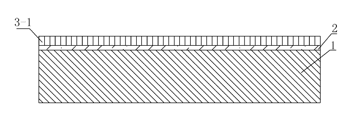
[0032] See figure 1 , (1) Make an adhesion layer 2 and a seed layer 3-1 on the surface of the wafer 1. The material of the adhesion layer can be one or more materials such as titanium, titanium nitride, tantalum, and tantalum nitride. The seed layer The material is copper;

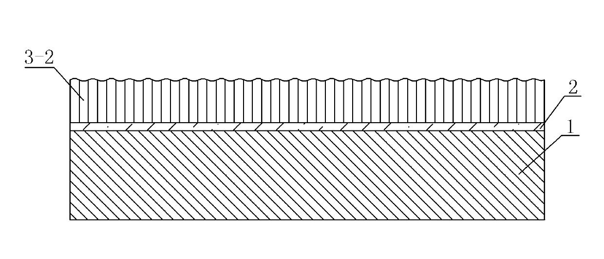
[0033] See figure 2 , (2) Deposit a copper layer 3-2 on the surface of the wafer by electroplating process, the thickness of the copper layer is 1-15 μm. Limited by the capability of the electroplating process itself, the roughness and flatness of the copper layer surface after electroplating are relatively poor;

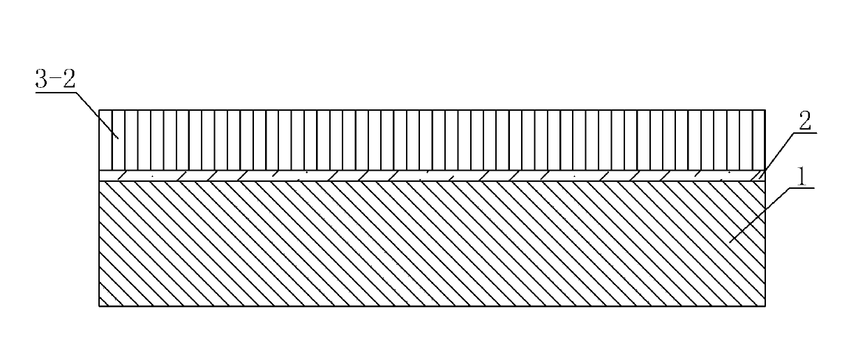
[0034] See image 3 , (3) Use chemical mechanical polishing technology to process the copper layer 3-2 on the wafer surface to improve the roughness and flatness of the copper surface, making it suitable for copper-copper bonding process;

[0035] See Figure 4 , (4) Patterning the copper lay...


PUM

PropertyMeasurementUnit
thicknessaaaaaaaaaa

Abstract

The invention provides a manufacturing method of copper-copper bonding salient points. The surface roughness of a copper cylinder is effectively reduced, the surface evenness of the micro salient points is improved, meanwhile, the consistency of the heights of the micro salient points in different areas of a wafer is guaranteed, and the requirements of a copper-copper bonding technology for the surface smoothness are met. The manufacturing method is characterized by including the following steps: (1) manufacturing an adhesion layer and a seed layer on the surface of the wafer, (2) depositing a copper layer on the surface of the wafer, (3) processing the copper layer on the surface of the wafer, and improving the surface roughness and the surface evenness of copper; (4) imaging the copper layer with a photolithography technique, (5) removing copper outside the positions of the micro salient points, and forming micro salient point structures on the wafer, (6) removing adhesion layer materials outside micro salient point areas of the surface of the wafer, and forming electrical isolation micro salient point structures, and (7) removing photoresist on the surface of the wafer, and obtaining the micro salient point structures with the even heights and the flat and smooth surfaces.

Description

technical field [0001] The invention relates to the technical field of microelectronic packaging, in particular to a method for manufacturing copper-copper bonding bumps. Background technique [0002] The current micro-bump manufacturing process uses photoresist to define the electroplating area after the seed layer is manufactured. Limited by the height of the micro-bumps, the thickness of the photoresist is relatively large, which leads to the insufficient capability of the traditional micro-bump manufacturing process in the production of small-sized micro-bumps. In addition, the copper-copper bonding process has strict requirements on the flatness of the bonding interface, and the electroplating process cannot meet its requirements. First of all, the surface roughness of the copper pillars produced by the electroplating process is relatively large, which cannot meet the requirements of copper-copper bonding for surface flatness; secondly, the flatness of the micro-bumps ...

Claims


Application Information

Patent Timeline
Patent Type & Authority Applications(China)
IPC IPC(8): H01L21/60
CPCH01L24/03H01L24/11
Inventor 薛恺于大全
Owner NAT CENT FOR ADVANCED PACKAGING
Why Eureka
Try Eureka