Lead frame and packaging structure forming methods

A technology of lead frame and packaging structure, which is applied in the field of semiconductor packaging, can solve the problems of low packaging efficiency, achieve the effects of improving packaging efficiency, increasing contact area, improving bonding strength and mechanical stability

Active Publication Date: 2014-04-23
NANTONG FUJITSU MICROELECTRONICS
View PDF5 Cites 16 Cited by
  • Summary
  • Abstract
  • Description
  • Claims
  • Application Information

AI Technical Summary

Problems solved by technology

[0004] Existing lead frame packages can only be packaged for a single

Method used


Image

  • Lead frame and packaging structure forming methods
  • Lead frame and packaging structure forming methods
  • Lead frame and packaging structure forming methods

Examples


Example Embodiment

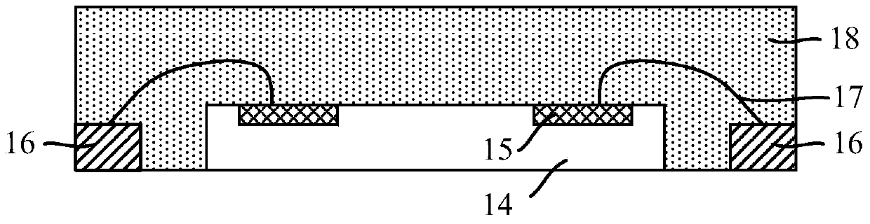
[0030] When encapsulating existing leadframes, please refer to the figure 1 First, the wafer needs to be cut to form semiconductor chips 14 one by one, and then metal wires 17 are formed through a wire bonding process. The metal wires 17 connect the pads 15 on the semiconductor chips 14 with the surrounding pins 16, and finally pass The plastic encapsulation material 18 encapsulates the semiconductor chip 14 and the pin 16. The existing packaging process can only realize the packaging of a single semiconductor chip and pin, and the encapsulation efficiency is low. In addition, the pins 16 are arranged around the semiconductor chip 14, and the pads 15 on the semiconductor chip 14 need to be electrically connected to the surrounding pins 16 through metal wires 17, so that the volume occupied by the entire packaging structure is relatively large. , which is not conducive to the improvement of the integration degree of the packaging structure.

[0031]The invention provides a met...


PUM


Abstract

The invention discloses lead frame and packaging structure forming methods. The packaging structure forming method comprises the following steps: a lead frame is provided, wherein the lead frame comprises a first surface and a second surface which is opposite to the first surface, the lead frame is provided with a plurality of bearing units which are arranged in a matrix manner and medium-strength ribs for fixing the bearing units, each bearing unit comprises a plurality of discrete pins, and a first opening is formed between every two neighboring pins; a first plastic packaged layer for filling the first openings is formed; an insulating layer is formed on the first surface of the lead frame and the surface of the first plastic packaged layer, wherein second openings for exposing surfaces of the pins are formed in the insulating layer; a plurality of semiconductor chips are provided, wherein each semiconductor chip is provided with a plurality of bonding pads, and metal bumps are formed on the bonding pads; and the plurality of semiconductor chip are arranged on the lead frame in a flipping manner, and the metal bumps on the semiconductor chips and the surfaces of the pins exposed out from the second openings are soldered together to form a plurality of packaging units which are arranged in a matrix manner. According to the method of the invention, the packaging efficiency can be improved.

Description

technical field [0001] The invention relates to the field of semiconductor packaging, in particular to a method for forming a lead frame and a packaging structure. Background technique [0002] With the development of electronic products such as mobile phones and notebook computers towards miniaturization, portable, ultra-thin, multimedia and low-cost to meet the needs of the public, high-density, high-performance, high-reliability and low-cost packaging forms and their Assembly technology has been rapidly developed. Compared with expensive packaging forms such as BGA (Ball Grid Array), new packaging technologies that have developed rapidly in recent years, such as Quad Flat No-lead Package (QFN) due to its good thermal performance and electrical The advantages of performance, small size, low cost and high productivity have triggered a new revolution in the field of microelectronic packaging technology. [0003] figure 1 It is a structural schematic diagram of an existing...

Claims


Application Information

Patent Timeline
IPC IPC(8): H01L21/48H01L21/50H01L21/60H01L21/56
CPCH01L2224/48091H01L21/4821H01L21/50H01L23/49544H01L23/49558H01L23/49586H01L24/81H01L2224/81H01L2224/16245H01L2924/00014
Inventor 陶玉娟
Owner NANTONG FUJITSU MICROELECTRONICS
Why Eureka
Try Eureka