Packaging structure

A technology of packaging structure and plastic sealing layer, which is applied in the direction of printed circuit, circuit, electric solid device, etc., can solve the problem of low packaging efficiency, achieve the effect of improving efficiency, meeting packaging requirements, and improving efficiency

Active Publication Date: 2014-04-23
NANTONG FUJITSU MICROELECTRONICS
View PDF7 Cites 15 Cited by
  • Summary
  • Abstract
  • Description
  • Claims
  • Application Information

AI Technical Summary

Problems solved by technology

[0004] The existing POP packaging technology has low packaging efficiency when forming a packaging structure

Method used


Image

  • Packaging structure
  • Packaging structure
  • Packaging structure

Examples


Embodiment Construction

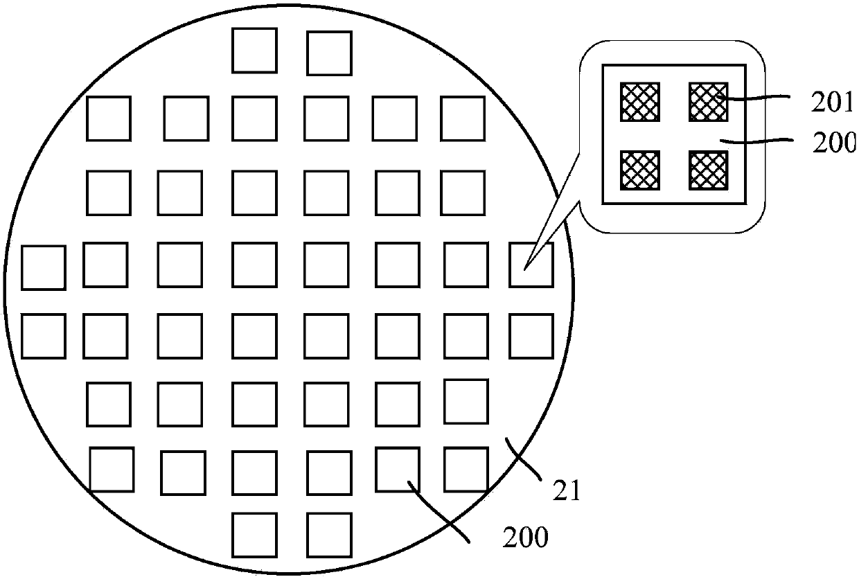
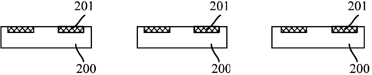
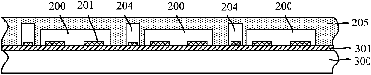
[0022] The existing POP packaging technology is to stack a single semiconductor chip on a circuit carrier, and the packaging efficiency is low.

[0023] For this reason, the present invention provides a package structure comprising a pre-sealing board, a plurality of semiconductor chips are packaged in the pre-sealing board, and the semiconductor chips on the pre-sealing board and the input pads of the circuit carrier are connected together by metal bumps , to realize the integrated packaging of multiple semiconductor chips and the circuit carrier, and improve the packaging efficiency.

[0024] In order to make the above objects, features and advantages of the present invention more comprehensible, specific embodiments of the present invention will be described in detail below in conjunction with the accompanying drawings. When describing the embodiments of the present invention in detail, for convenience of explanation, the schematic diagrams will not be partially enlarged ac...


PUM


Abstract

The invention discloses a packaging structure. The packaging structure comprises: a circuit carrier board, wherein the circuit carrier board comprises a first surface and a second surface which is opposite to the first surface, the circuit carrier board is provided with a plurality of bearing units which are arranged in a matrix manner, first surfaces of the bearing units are provided with a plurality of input bonding pads, second surfaces of the bearing units are provided with a plurality of output bonding pads, and the input bonding pads and the output bonding pads are connected through an interconnection structure; a pre-packaged panel, wherein the pre-packaged panel comprises a first plastic packaged layer, a plurality of integrated unit which are arranged in a matrix manner are arranged in the first plastic packaged layer, at least one semiconductor chip is arranged in each integrated unit, surfaces of the semiconductor chips are provided with a plurality of bonding pads, the bonding pads are provided with first metal bumps, the pre-packaged panel is arranged on the first surface of the circuit carrier board in a flipping manner, and the first metal bumps and the input bonding pad are soldered together; a filling layer for filling the space between the first surfaces of the bearing units and the pre-packaged panel; and second metal bumps located on the output bonding pads of the second surfaces of the bearing units. According to the packaging structure of the invention, the integration level is improved.

Description

technical field [0001] The invention relates to the field of semiconductor packaging, in particular to a packaging structure. Background technique [0002] With the development of electronic products such as mobile phones and notebook computers towards miniaturization, portable, ultra-thin, multimedia and low-cost to meet the needs of the public, the traditional single-chip packaging technology can no longer meet the increasingly novel market demand. Packaging technology with light, thin, short and small product characteristics, high density and low cost has become the mainstream of market research. Among the various packaging technologies at present, POP (package on package) and PIP (package in package) packaging technologies are typical representatives. [0003] Taking the POP packaging technology as an example, the volume and thickness of the entire packaging structure can be reduced by stacking semiconductor chips on a circuit carrier. [0004] The packaging efficiency...

Claims


Application Information

Patent Timeline
Patent Type & Authority Applications(China)
IPC IPC(8): H01L23/31H01L23/488
CPCH01L24/19H01L24/96H01L21/568H01L24/97H01L2224/12105H01L2224/16225H01L2224/24195H01L2224/32225H01L2224/73204H01L2224/97H01L2924/15311H01L2924/15788H01L23/3114H01L23/3128H01L2924/19105H01L2924/3511H01L25/16H01L2224/81H01L2924/00H01L25/10H05K1/113H05K1/181H05K2201/10234H05K2201/1031H05K2201/10378H05K2201/10522H05K2201/10962H05K2201/10977
Inventor 陶玉娟
Owner NANTONG FUJITSU MICROELECTRONICS
Why Eureka
Try Eureka