Processing method for reusing unqualified chamfered silicon briquette

A processing method and technology for silicon blocks, which are applied in stone processing equipment, fine working devices, manufacturing tools, etc., can solve the problems of scrapping, slurry interruption, and increase in manufacturing costs, and achieve unique processing methods, reduce raw material waste, and reduce waste. The effect of improving utilization

Active Publication Date: 2014-04-30
YINGLI ENERGY CHINA
View PDF7 Cites 10 Cited by
  • Summary
  • Abstract
  • Description
  • Claims
  • Application Information

AI Technical Summary

Problems solved by technology

[0003] However, in the actual production process of monocrystalline silicon ingots, due to the interruption of the slurry flow or the steel wire skipping during the multi-wire cutting process, there will occasionally be accidents where the size of the silicon ingot is not qualified.
The frequency of such processing abnormalities is not high, but once they occur, the loss of silicon blocks is very serious
Analyzing the characteristics of this type of silicon block, the most problematic problem is that the chamfering is unqualified, such as figure 1 As shown, the circle represents the outer circle of the monocrystalline silicon rod, and the straight line represents the steel wire. figure 1 A is the end face of the silicon block that is qualified for normal cutting and chamfering, figure 1 B is the end face of the silicon block with unqualified chamfering. Due to the overall offset of the wafer, the dimensions of the four corners of the end face are inconsistent, and the chamfering size of the silicon block is unqualified.
[0004] At present, such unqualified silicon blocks can no longer be cut into silicon wafers, and can only be directly scrapped as recycled materials
Obviously, this is a huge waste, and direct scrapping will inevitably lead to an increase in manufacturing costs

Method used


Image

  • Processing method for reusing unqualified chamfered silicon briquette
  • Processing method for reusing unqualified chamfered silicon briquette
  • Processing method for reusing unqualified chamfered silicon briquette

Examples


Embodiment Construction

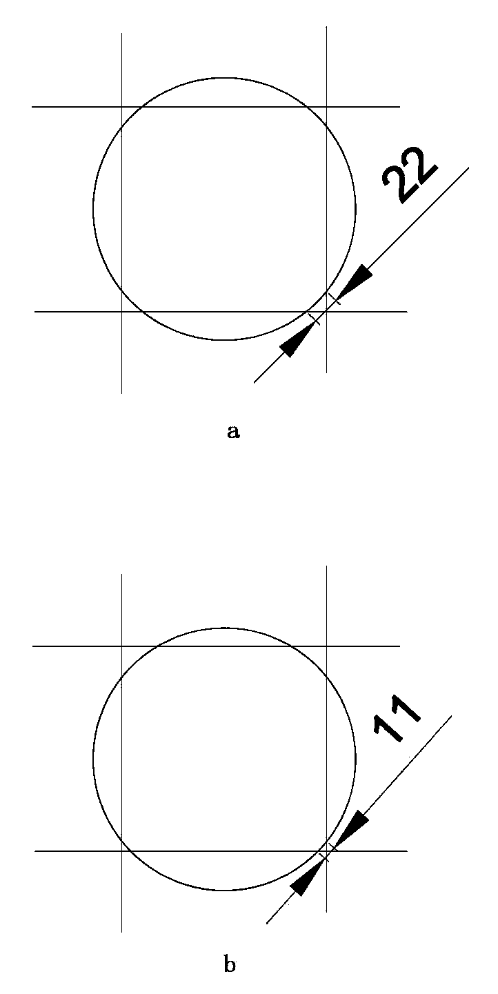
[0026] like figure 1 As shown, the circle represents the outer circle of the single crystal silicon rod, the straight line represents the steel wire, figure 1 a is the end face of the silicon rod that is qualified for normal cutting and chamfering. At this time, the four chamfers are equal, and the radians are all 22. figure 1 b is the end face of the silicon rod with unqualified chamfer. Due to the overall offset of the silicon rod, the dimensions of the four chamfers on the end face are inconsistent. In the prior art, figure 1 The cut and unqualified silicon blocks shown in b can only be scrapped, which will cause serious waste of raw materials and increase the cost of qualified silicon blocks.

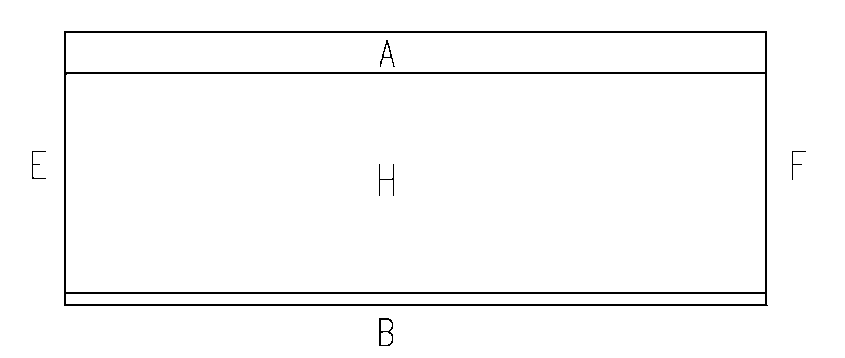
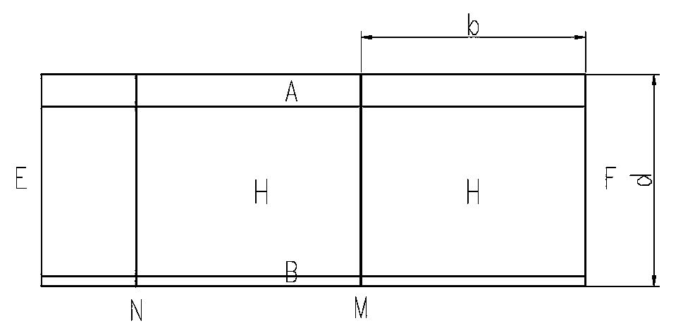
[0027] figure 2 Shown is the structural schematic diagram of the unqualified silicon wafer, figure 1 Shown is the structure viewed from the end face of the ingot, figure 2 For the structure viewed from the side of the ingot, image 3 for figure 2 left view of , in figure...


PUM


Abstract

The invention discloses a processing method for reusing an unqualified chamfered silicon briquette, and belongs to the field of semiconductor device processing. The silicon briquette is firstly cut in the direction parallel to the end face of the unqualified silicon briquette, small cuboid-shaped silicon briquettes are obtained, and the length of the small silicon briquettes is larger than the edge length of the end face. Then, the small cuboid-shaped silicon briquettes are processed to be small cube-shaped silicon briquettes, and the side faces of the small cube-shaped silicon briquettes are opposite and are pasted to form a new strip-shaped silicon briquette. Then, rolling chamfering is carried out on the new strip-shaped silicon briquette, a qualified silicon single crystal rod is obtained, and finally the silicon single crystal rod can be cut into qualified silicon wafers. According to the method, the unqualified chamfered silicon briquette can be processed and reused, the silicon wafers with the qualified size can be obtained in a cutting mode, the method can greatly lower raw material waste caused by unqualified chamfering and improve the use ratio of materials, and silicon wafer cost is greatly lowered. The method is novel in thought and unique and simple in treatment mode, technicists in the field can understand the method through one glance, and the method is very suitable for being popularized in a wide range, and can achieve good economic benefits.

Description

technical field [0001] The invention belongs to the technical field of semiconductor device processing. Background technique [0002] At present, the entire solar energy manufacturing industry is in a period of reducing costs and innovating processing technologies in various links to improve product competitiveness. Among them, the field of silicon wafer cutting has always been the highlight of cost reduction. Several main processing processes in this cutting and manufacturing process are: first, the single crystal silicon rod is processed into a rectangular silicon block with a square end face by multi-line cutting by the square root equipment, and then the edges of the silicon block are ground one by one by the grinding equipment. Polishing and chamfering, the last step is the bonding process to position and bond the processed silicon block on a specific tray. After the glue is dry, it is processed by a multi-wire cutting machine. [0003] However, in the actual productio...

Claims


Application Information

Patent Timeline
Patent Type & Authority Applications(China)
IPC IPC(8): B28D5/00
Inventor 李双江郭钊甄云云
Owner YINGLI ENERGY CHINA
Why Eureka
Try Eureka