

ESD transient state detection circuit
A detection circuit, transient technology, applied in the field of electronics, can solve the problems of occupation, large chip area, etc., to achieve the effect of reducing manufacturing costs, prolonging the conduction time, and improving the uniformity of output voltage
- Summary
- Abstract
- Description
- Claims
- Application Information
AI Technical Summary
Problems solved by technology
Method used
Image

Examples
Embodiment 1
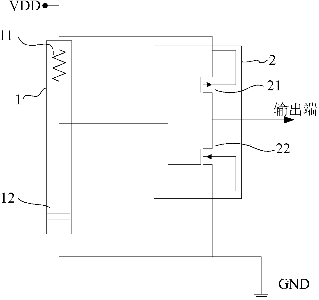
[0022] Such as image 3 As shown, the structure diagram of this example includes: drive network 1; control network 2; feedback network 3. The drive network 1 includes a drive resistor 11; one end of the drive resistor is connected to the power rail, the other end is connected to the drive capacitor 12 and then the input end of the control network 2, and the other end of the drive capacitor is connected to GND. The control network 2 includes an inverter PMOS tube 21; an inverter NMOS tube 22. The gate of the inverter PMOS tube 21 and the inverter NMOS tube 22 are connected as the input terminal of the control network 2, and the drain is connected as the output terminal of the control network 2. The source of the inverter PMOS transistor 21 is connected to the substrate and connected to the power supply VDD. The source of the inverter NMOS tube 22 is connected to the substrate and connected to GND. The feedback network 3 includes a feedback NMOS transistor 32; a feedback resist...
Embodiment 2
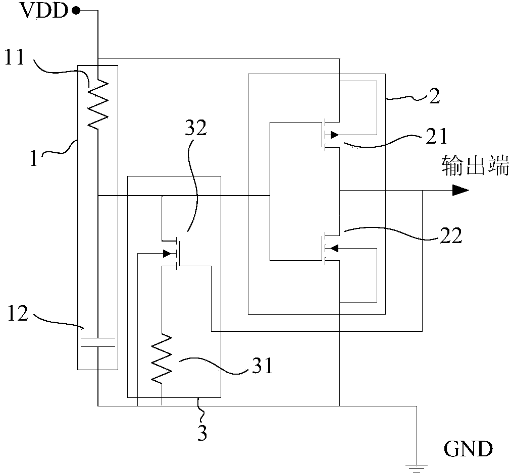
[0029] Such as Figure 4 As shown, the difference from Embodiment 1 is that only the substrate of the feedback NMOS transistor 32 in Embodiment 1 is connected to its source. Specifically include: drive network 1; control network 2; feedback network 3. The drive network 1 includes a drive resistor 11; one end of the drive resistor is connected to the power supply VDD, the other end is connected to the drive capacitor 12 and then the input end of the control network 2, and the other end of the drive capacitor is connected to GND. The control network 2 includes an inverter PMOS tube 21; an inverter NMOS tube 22. The gate of the inverter PMOS tube 21 and the inverter NMOS tube 22 are connected as the input terminal of the control network 2, and the drain is connected as the output terminal of the control network 2. The source of the inverter PMOS transistor 21 is connected to the substrate and connected to the power supply VDD. The source of the inverter NMOS tube 22 is connected...
Embodiment 3
[0032] Such as Figure 5 As shown, the difference from the first embodiment is that the feedback NMOS transistor 32 in the first embodiment only needs to be replaced with an NPN transistor 33. The collector of the NPN transistor is connected to the input end of the control network 2, the emitter is connected to one end of the feedback resistor 31, and the other end of the feedback resistor 31 is grounded. The base of the NPN transistor 33 is connected to the output terminal of the control network 2. Specifically include: drive network 1; control network 2; feedback network 3. The drive network 1 includes a drive resistor 11; one end of the drive resistor is connected to the power supply VDD, the other end is connected to the drive capacitor 12 and then the input end of the control network 2, and the other end of the drive capacitor is connected to GND. The control network 2 includes an inverter PMOS tube 21; an inverter NMOS tube 22. The gate of the inverter PMOS tube 21 and ...
PUM
 Abstract
Description
Claims
Application Information