Active resonant circuit with resonant-frequency tunability

a resonant frequency and active resonant technology, applied in the field of wireless communication circuits, can solve the problems of long time required large occupied area, and inability to switch the frequency of local signals in a few seconds, and achieve the effect of small chip occupied area and low power consumption

Inactive Publication Date: 2009-02-05
RENESAS ELECTRONICS CORP
View PDF2 Cites 26 Cited by
  • Summary
  • Abstract
  • Description
  • Claims
  • Application Information

AI Technical Summary

Benefits of technology

[0029]Effects obtained by the representative ones of the inventions disclosed in the specification will be briefly described

Problems solved by technology

However, since the PLL is realized by forming a negative feedback loop, there is a drawback that the time required to switch the frequencies of local signals is long, and it

Method used


Image

  • Active resonant circuit with resonant-frequency tunability
  • Active resonant circuit with resonant-frequency tunability
  • Active resonant circuit with resonant-frequency tunability

Examples


Embodiment Construction

Representative Embodiments

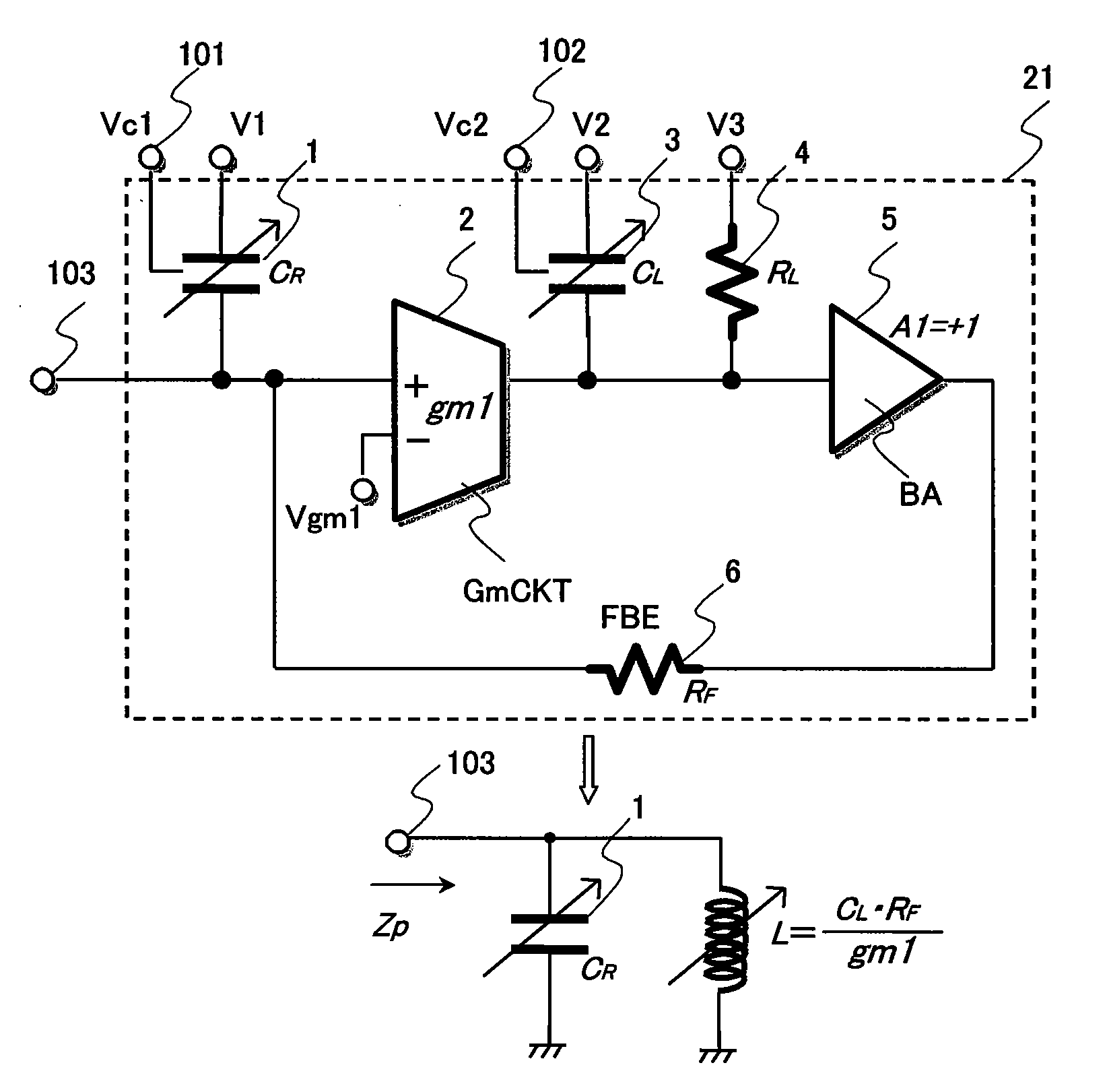
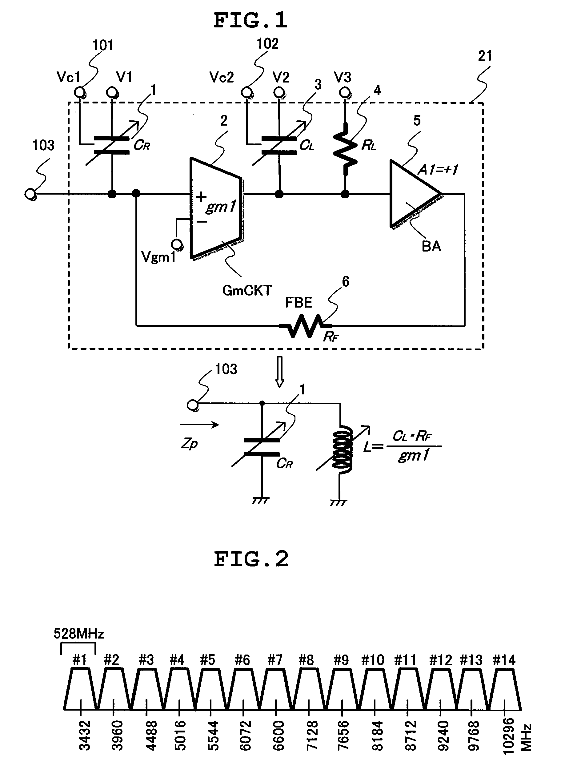
[0054]First, outline of representative embodiments of the present invention disclosed in the specification will be described. Reference numerals in the diagram in parenthesis used for describing outline of the representative embodiments merely indicate components included in the concept.[0055](1) A semiconductor integrated circuit as a representative embodiment of the present invention includes, on a semiconductor chip, a resonant circuit including a first capacitor (1) having a capacitance (CR) which can be controlled by a first control signal (Vc1) applied to a first control terminal (101), and a gyrator (2, 5) for equivalently emulating an inductor (L) by including a second capacitor (3) having a capacitance (CL) which can be controlled by a second control signal (Vc2) applied to a second control terminal (102) (refer to FIG. 1).

[0056]According to the embodiment, the resonant circuit is realized by not a spiral inductor having a large chip occupied area ...


PUM


Abstract

The present invention is directed to provide a low-power-consumption wide-range RF signal processing unit having a small chip occupation area. A semiconductor integrated circuit has, on a semiconductor chip, a resonant circuit including a first capacitor having a capacitance which can be controlled by a first control signal of a first control terminal, and a gyrator for equivalently emulating an inductor by including a second capacitor having a capacitance which can be controlled by a second control signal of a second control terminal. The capacitance and the inductor form a parallel resonant circuit. At the time of changing parallel resonant frequency, the capacitances of the first and second capacitors are coordinately changed. The parallel resonant circuit is suitable for an active load which is connected to an output node of an amplifier.

Description

CLAIM OF PRIORITY[0001]The present application claims priority from Japanese application JP 2007-197631 filed on Jul. 30, 2007, the content of which is hereby incorporated by reference into this application.FIELD OF THE INVENTION[0002]The present invention relates to a wireless communication circuit as a component of a wireless communication system and, more particularly, to a technique effectively applied to a method of transmitting / receiving data using a wide multiband.BACKGROUND OF THE INVENTION[0003]Generally, a wireless communication system uses a predetermined RF band for transmitting / receiving data. For example, in IEEE802.11g known as an American standard of a local area network (LAN), the RF band of 2.4 GHz to 2.47 GHz is used and 54 Mbps is achieved as the maximum data rate in the range of the communication distance of 50 m to 100 m.[0004]However, demands for data of general users are increasing year by year. It is strongly desired to download not only high definition imag...

Claims


Application Information

Patent Timeline
IPC IPC(8): H03H11/00
CPCH03H11/42H03H11/1291H03H11/0472
Inventor MASUDA, TORUMORI, HIROSHI
Owner RENESAS ELECTRONICS CORP
Why Eureka
Try Eureka