Gain bootstrap type C class reverser and application circuit thereof

A technology of inverters and resistors, which is applied to parts, electrical components, and electric pulses of circuits that generate electric pulses. It can solve the problem of large influence of steady-state characteristics, dynamic characteristics, establishment time and dynamic power consumption process deviation, and application circuit performance. Problems such as degradation, loss of function, etc., to ensure robustness and practicability, reduce chip footprint, and improve effectiveness

Inactive Publication Date: 2010-04-07
ZHEJIANG UNIV
View PDF0 Cites 20 Cited by
  • Summary
  • Abstract
  • Description
  • Claims
  • Application Information

AI Technical Summary

Problems solved by technology

[0009] The technical problem to be solved by the present invention is to provide a gain bootstrap type C class inverter to overcome the low self-gain of the class C inverter in the prior art, which is difficult to be used in occasions requiring higher gain, and The steady-state characteristics (gain, bandwidth,

Method used


Image

  • Gain bootstrap type C class reverser and application circuit thereof
  • Gain bootstrap type C class reverser and application circuit thereof
  • Gain bootstrap type C class reverser and application circuit thereof

Examples


Example Embodiment

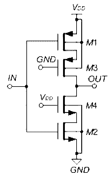
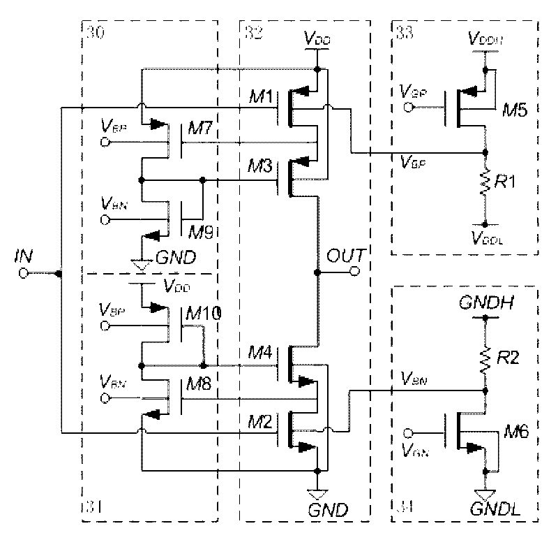
[0048] Embodiment 1: The circuit structure diagram of the gain bootstrap type C class inverter proposed by the present invention is as attached image 3 As shown, in addition to the class C inverter module 32 of the prior art, it also includes gain bootstrap modules 30, 31 and body potential modulation modules 33, 34.

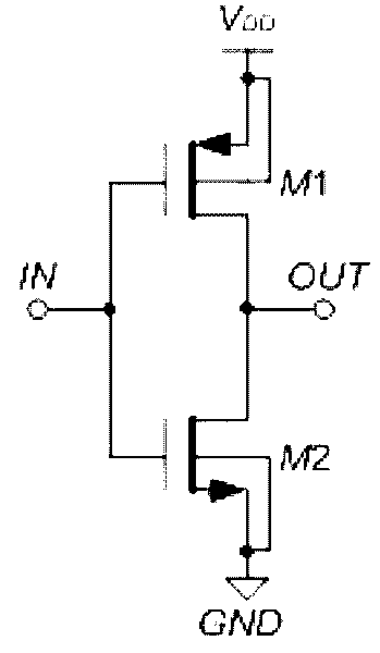
[0049] The class C inverter 32 in the prior art is composed of I / OPMOS transistors M1, M3 and I / O NMOS transistors M2, M4, wherein M1 and M2 are input transistors of the inverter. The power supply voltage V of the class C inverter 32 in the prior art DD Slightly lower than the sum of the threshold voltages of M1 and M2, it can realize two different working states of high gain, low power consumption and high slew rate and high current according to the difference in the bias voltage of the input terminal. The details are as follows:

[0050] Assuming that the threshold voltages of M1 and M2 are approximately equal, when the input signal is a common-mode voltage ...

Example Embodiment

[0071] Embodiment 2: The pseudo-differential structure switched capacitor integrator proposed by the present invention is as attached Figure 4 As shown, it includes two gain bootstrap type C-type inverters 40 and a common-mode feedback circuit 41 of the prior art, a sampling capacitor C S , compensation capacitor C C , Integrating capacitance C I and switch. Among them, two gain bootstrap type C class inverters 40 are respectively located in the forward and negative branches of the integrator, and the two inverters are differentially symmetrical to form a pseudo-differential structure, while two common-mode feedback circuits 41 are respectively located in the integrator The positive and negative legs form a common-mode feedback.

[0072] In actual work, the switched capacitor integrator is divided into sampling phase and integrating phase, which are controlled by two non-overlapping clocks of p1 and p2, as shown in the attached Figure 5 As shown, the integral phase can b...

Example Embodiment

[0081] Embodiment 3: The 2-1 cascaded Sigma-Delta analog-to-digital converter proposed by the present invention includes a pseudo-differential switched capacitor integrator based on a gain-bootstrap class-C inverter. In order to illustrate the specific structure and working mode of the 2-1 cascaded Sigma-Delta analog-to-digital converter, let's start with the general structure and working mode of the Sigma-Delta analog-to-digital converter:

[0082] The structural block diagram of the Sigma-Delta analog-to-digital converter is attached Image 6 As shown, it includes an anti-aliasing filter 60 , a sample-and-hold 61 , an analog modulator 62 and a digital decimation filter 63 . The analog modulator 62 is used for noise shaping in the analog-to-digital conversion process, and it includes loop filter 65, feedforward ADC (analog-to-digital converter) 66, feedback DAC (digital-to-analog converter) 67, adder 64 and other parts, The feed-forward ADC66 and the feedback DAC67 are colle...


PUM


Abstract

The invention discloses a gain bootstrap type C class reverser and an application circuit thereof. Based on a C class reverser 32 in the prior art, the gain bootstrap type C class reverser is additionally provided with micropower gain bootstrap modules 30 and 31 and bulk potential modulation modules 33 and 34, wherein the gain bootstrap modules 30 and 31 greatly improve the steady-state gain of the C class reverser under the condition of not losing the output swing or increasing the circuit power consumption significantly so as to improve the integral precision of a gain bootstrap type C class reverser-based pseudo-differential structure switched capacitor integrator and the analog-to-digital conversion precision of an analog-to-digital converter, and broaden the application range of the C class reverser; and the bulk potential modulation modules 33 and 34 make the steady-state characteristics (gain, bandwidth, static power consumption and the like) and the dynamic characteristics (slew rate, setting time, dynamic power consumption and the like) of the whole reverser consistent under the condition of different corners, and greatly improve the stability and the robustness of the application circuit of the gain bootstrap type C class reverser under the condition of not increasing the power consumption significantly.

Description

[0001] technical field [0002] The invention relates to a class-C inverter and an application circuit thereof, belonging to the technical field of integrated circuits. Background technique [0003] In traditional analog circuit design, the operational amplifier is the main functional module, and it is widely used in sample-and-hold, algebraic operations, common-mode feedback, and buffer circuits. At the same time, the operational amplifier is also the main power consumption module in the analog circuit. At present, low voltage and low power consumption are the mainstream trend in the development of analog circuit design, but for operational amplifiers, the reduction of power supply voltage means the reduction of dynamic range, the reduction of input common mode range, the increase of capacitance and the inability to turn on or off the floating circuit. Switches, etc., we need to use more sophisticated circuit design to overcome these difficulties. Therefore, how to implemen...

Claims


Application Information

Patent Timeline
IPC IPC(8): H03K3/01H03K3/356
Inventor 罗豪韩雁黄小伟蔡坤明张昊韩晓霞
Owner ZHEJIANG UNIV
Why Eureka
Try Eureka