Array substrate as well as production method thereof and display device

A technology for array substrates and base substrates, applied in the fields of array substrates, array substrates, and display devices, can solve problems such as liquid crystal deflection disorder in display devices, affect the display quality of display devices, and liquid crystal deflection disorder in display devices, etc., to achieve improved Transmittance, avoiding light leakage and color mixing, and improving display quality

Inactive Publication Date: 2014-05-07
BOE TECH GRP CO LTD
View PDF5 Cites 7 Cited by
  • Summary
  • Abstract
  • Description
  • Claims
  • Application Information

AI Technical Summary

Problems solved by technology

When the size of the pixel area is getting smaller and smaller, in order to keep the pixel area with a certain aperture ratio, the current spacing between adjacent electrodes (that is, figure 1 and figure 2 The d) in d) becomes smaller and smaller, so that when the display device including the array substrate is driven, the electric field between adjacent electrodes will interfere with each other, so that the liquid crystal deflection of the display device is disordered, which may cause light leakage and color mixing of the display device , seriously affecting the display quality of the display device; for example, if image 3 As shown, taking the electrode 30 above the data line 20 as a pixel electrode, and the distance between adjacent pixel electrodes is 10 microns (that is, d=10 microns) as an example, the light leakage of the array substrate is tested, according to the test As a result, it can be seen that liquid crystal a, which should not be deflected, is deflected, causing light leakage on the array substrate at the corresponding position of liquid crystal a.
[0004] To sum up, at present, for high-resolution array substrates, the electric fields between adjacent electrodes contained in them will interfere with each other, causing the liquid crystal deflection of the display device including the array substrate to be chaotic, which may cause light leakage and color mixing of the display device, seriously affecting The display quality of the display device

Method used


Image

  • Array substrate as well as production method thereof and display device
  • Array substrate as well as production method thereof and display device
  • Array substrate as well as production method thereof and display device

Examples


Embodiment approach 1

[0062] Preferably, the first transparent electrode is in the shape of a slit, and the second transparent electrode is in the shape of a plate.

[0063] Preferably, the second transparent electrode is located in a different layer from the first transparent electrode.

[0064] For example, for the ADS (Advanced Smart Display System, advanced ultra-dimensional field switching technology) mode, when the first transparent electrode is in the shape of a slit, the second transparent electrode can be in the shape of a plate; and, the second transparent electrode and the first transparent electrode on different floors.

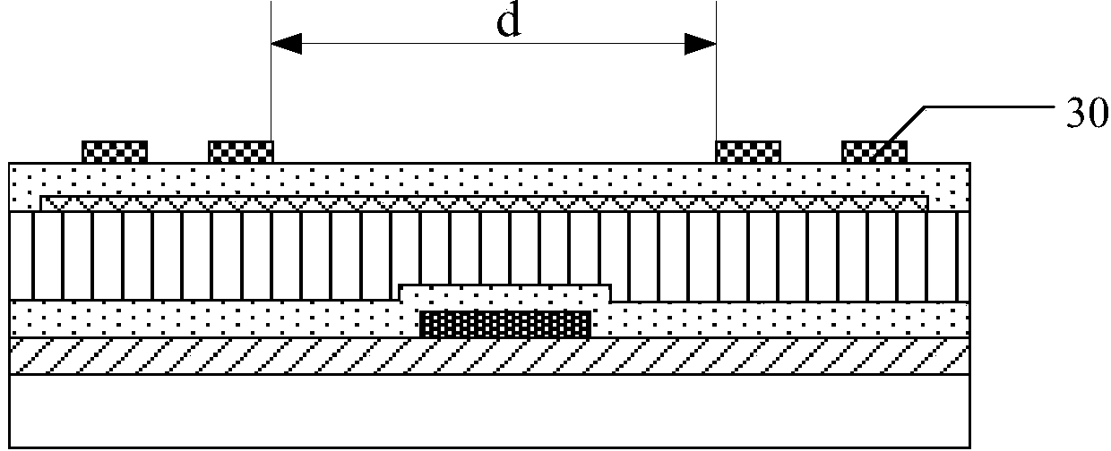
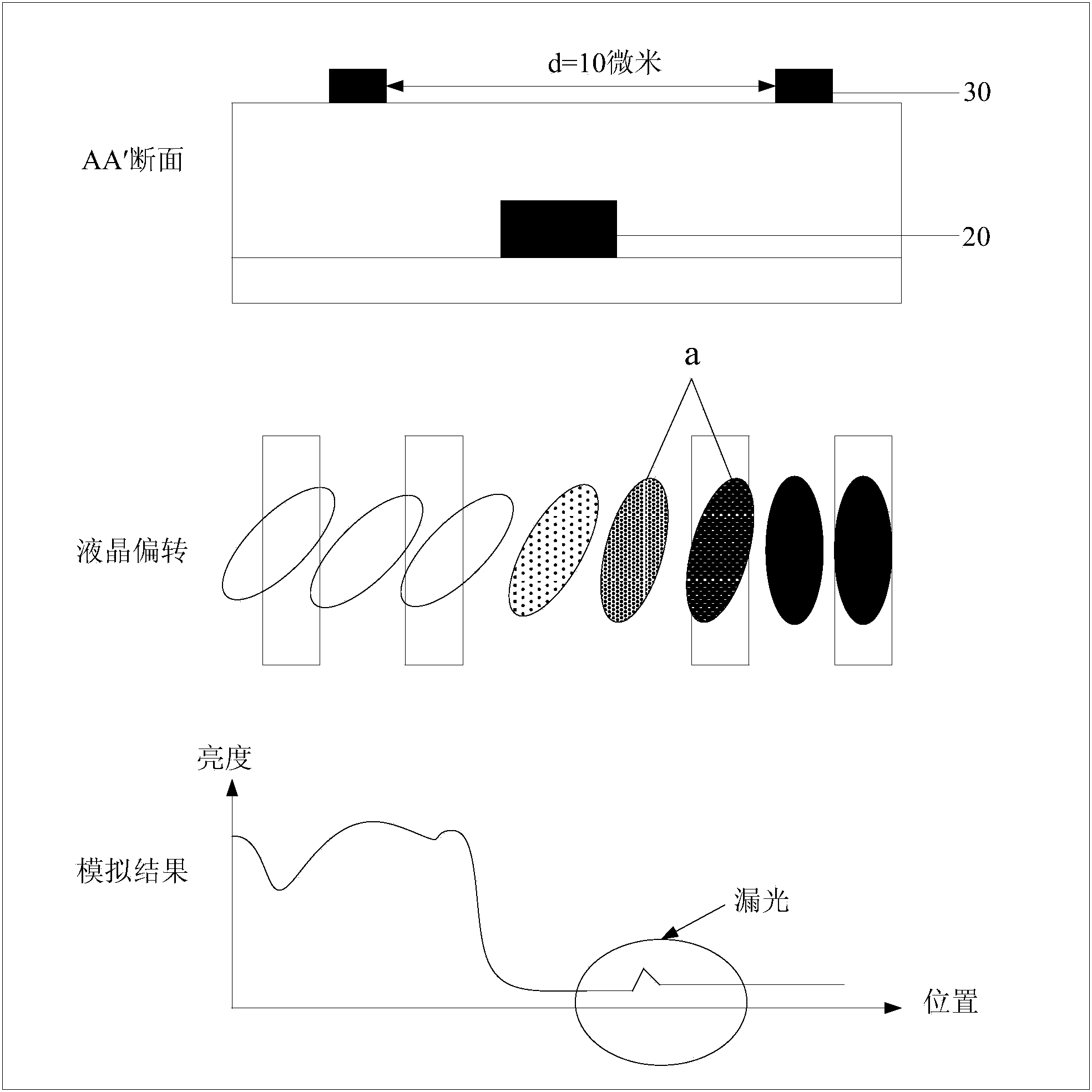
[0065] ADS technology is to form a multi-dimensional electric field through the electric field generated by the edge of the slit electrode in the same plane and the electric field generated between the slit electrode layer and the plate electrode layer, so that all the oriented liquid crystal molecules between the slit electrodes and directly above the electrodes in th...

Embodiment approach 2

[0073] Preferably, the first transparent electrode is in the shape of a slit, and the second transparent electrode is in the shape of a slit.

[0074] Preferably, the second transparent electrode is located on a different layer from the first transparent electrode, or

[0075] The second transparent electrodes are located on the same layer as the first transparent electrodes, and the second transparent electrodes and the first transparent electrodes are arranged crosswise.

[0076] In a specific implementation, when the second transparent electrodes are located in different layers from the first transparent electrodes, an insulating member may be provided between adjacent second transparent electrodes, or the insulating member may not be provided.

[0077] Preferably, when the second transparent electrode and the first transparent electrode are located in different layers, the insulating component is located between two adjacent second transparent electrodes, and the upper sur...

Embodiment 1

[0173] In Embodiment 1 of the present invention, the first transparent electrode is a pixel electrode, and the second transparent electrode is a common electrode, and the first transparent electrode is in the shape of a slit, and the second transparent electrode is in the shape of a plate.

[0174] Preferably, the manufacturing method of the array substrate in the embodiment of the present invention includes:

[0175] Step A1, forming gates and gate lines on the base substrate;

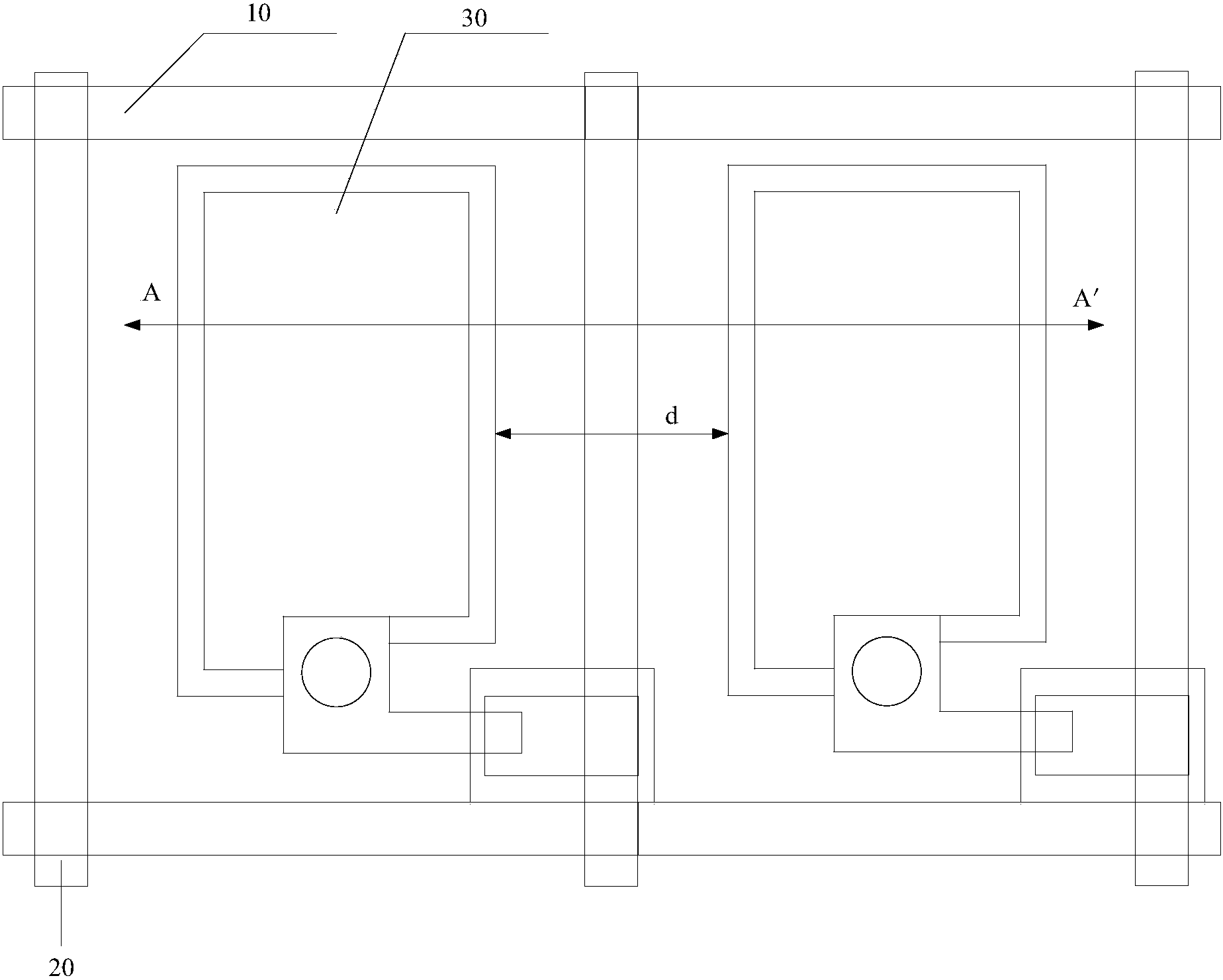
[0176] Among them, such as Figure 5A As shown, the formed gate 1 and gate line 10 are connected to each other.

[0177] Step A2, forming a gate insulating layer covering the gate and gate lines on the base substrate;

[0178] Step A3, forming an active layer on the gate insulating layer;

[0179] Among them, such as Figure 5A As shown, the formed gate 1 completely covers the active layer 2 .

[0180] Step A4, forming source electrodes, drain electrodes and data lines on the active layer;

[01...


PUM


Abstract

The invention relates to the technical field of the display, in particular to an array substrate, a display device and a production method of the array substrate, which is used for reducing the interference of an electric field between two adjacent first transparent electrodes of the array substrate. The array substrate comprises an underlayer substrate, a plurality of grid lines, a plurality of data lines and first transparent electrodes, wherein the grid lines and the data lines are arranged on the underlayer substrate and intersected with one another to define pixel areas, each first transparent electrode is arranged in each pixel area, and the array substrate also comprises insulation parts; each insulation part is arranged between every two adjacent first transparent electrodes, the upper surface of each insulation part is higher than the upper surface of the first transparent electrode, and the lower surface of each insulation part is lower than the upper surface of the first transparent electrode. By adopting the array substrate, the interference of the electric field between two adjacent first transparent electrode can be reduced.

Description

technical field [0001] The present invention relates to the field of display technology, in particular to an array substrate, a display device, and a method for manufacturing the array substrate. Background technique [0002] The array substrate of the display device includes a base substrate, a plurality of gate lines and data lines on the base substrate intersecting each other to define pixel areas, and electrodes located in each of the pixel areas. by figure 1 For example, such as figure 1 As shown, two gate lines 10 and three data lines 20 intersect each other to define two pixel areas, and an electrode 30 is arranged in each pixel area, wherein, taking the electrode 30 as a pixel electrode as an example, figure 2 The structure diagram described is figure 1 The cross-sectional view of the array substrate shown in the AA' direction, such as figure 2 As shown, two adjacent electrodes 30 are located on the same layer with a certain distance between them. [0003] At ...

Claims


Application Information

Patent Timeline
Patent Type & Authority Applications(China)
IPC IPC(8): G02F1/1333G02F1/1343
CPCG02F1/134363G02F1/136286G02F2201/40G02F1/13606H01L27/124H01L27/1259G02F1/133345G02F1/133512G02F1/133514G02F1/13439H01L21/28
Inventor 张锋曹占锋姚琪
Owner BOE TECH GRP CO LTD
Why Eureka
Try Eureka