Double-sided conductive transparent film
A conductive transparent film, double-sided technology, applied in the field of conductive layer, can solve the problems that affect the display brightness, contrast and color, the light transmittance of the conductive film is not very high, and the power consumption of equipment increases, so as to achieve the improvement of yield rate and power consumption The effect of low volume and cost reduction
- Summary
- Abstract
- Description
- Claims
- Application Information
AI Technical Summary
Problems solved by technology
Method used
Image
Examples
Embodiment 1
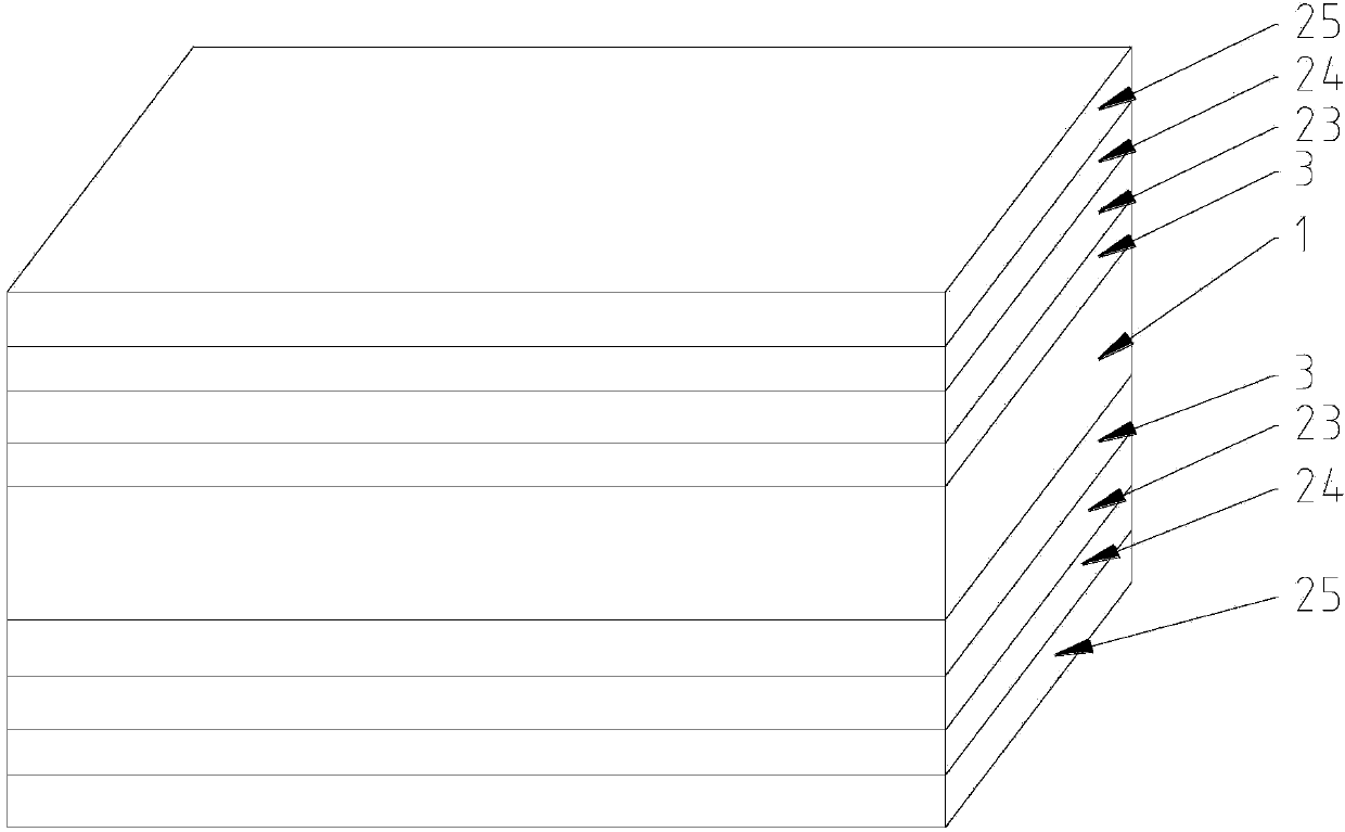
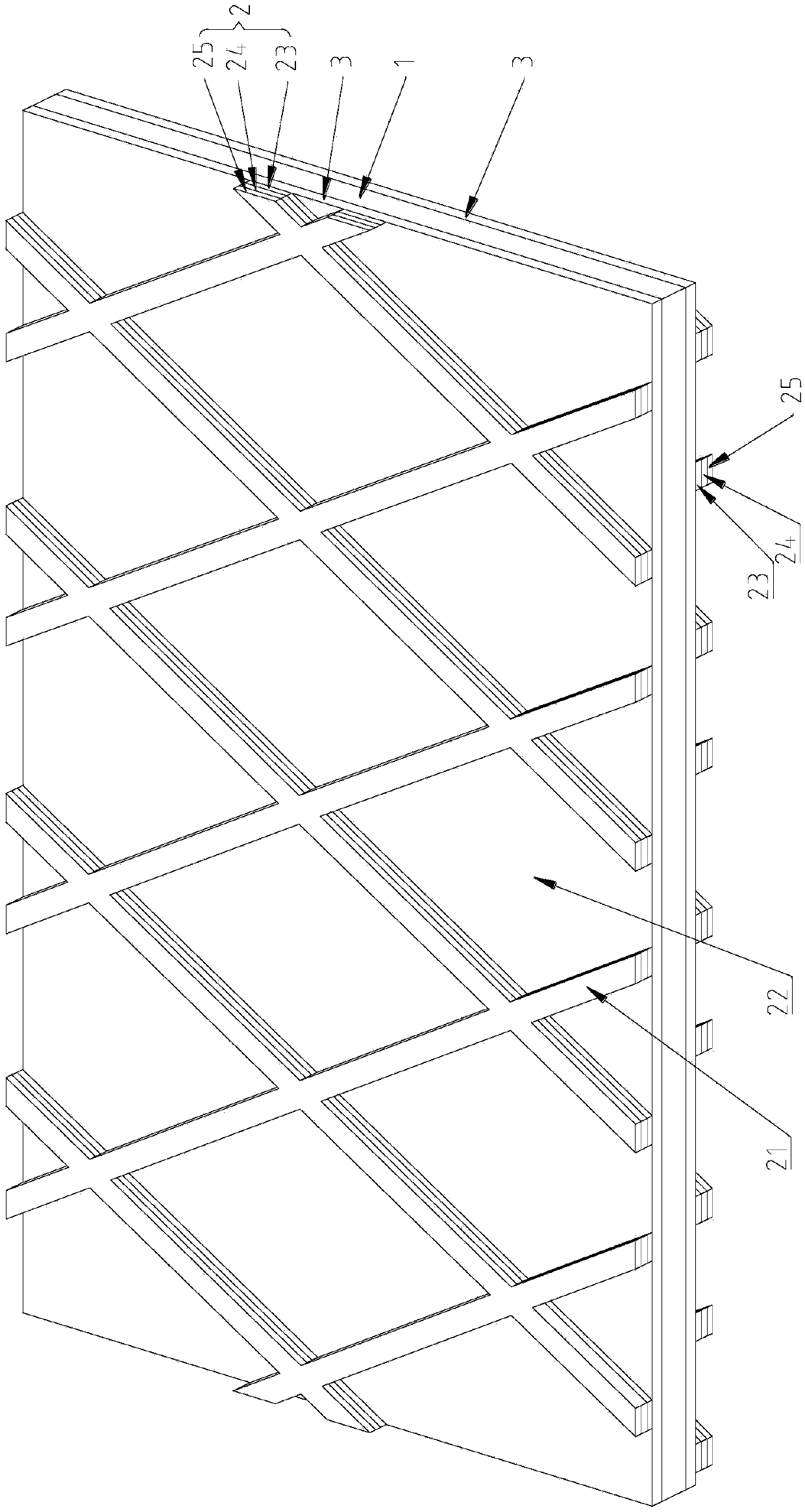
[0026] Embodiment 1: as figure 1 As shown, a double-sided conductive transparent film includes a protective layer 25, a conductive layer 24, a black layer 23, a bottom layer 3, a substrate 1, a bottom layer 3, a black layer 23, a conductive layer 24, and a protective layer 25 from bottom to top. , the substrate 1 is glass or a transparent plastic film, which includes a first surface and a second surface opposite to each other, and the first surface and the second surface of the substrate 1 are respectively coated by vacuum sputtering or evaporation coating Overlay the bottom layer 3, the bottom layer 3 is transparent SiO 2 Ink can be sprayed on the first surface and the second surface to form an ink pattern; then a black layer 23, a conductive layer 24 and a protective layer 25 are sequentially plated on the bottom layer 3, wherein the black layer 23 is a metal oxide layer, preferably oxidized The mixture of chromium and nickel oxide has a thickness of 40nm-100nm, and ...
Embodiment 2
[0028] Embodiment 2: the present invention provides another kind of double-sided transparent conductive film, and present embodiment is compared with embodiment 1, and protective layer 25 is changed into metal oxide layer, the mixture of preferred chromium oxide and nickel oxide, and it also can play To prevent oxidation, so that the naked eye can also observe from the other side.
[0029] In the present invention, a black layer, a conductive layer, and a protective layer are respectively plated on both sides of the substrate, and etched to form a metal grid, that is, both sides of the transparent film are metal grids, and the metal grid lines are used instead of ITO, which can not only reduce the impedance , reduce costs, and have good light transmittance; in addition, two films were used to be laminated to form a capacitive touch screen, but now only one film is required, which reduces the cost of one film and the adhesive used for bonding, and the cost is significantly r...
PUM
 Abstract
Description
Claims
Application Information

