Array substrate, display device and array substrate manufacturing method

A technology of an array substrate and a manufacturing method, applied in the field of liquid crystal display, can solve problems such as high cost and complicated process, and achieve the effects of reducing process cost, simplifying manufacturing process, and reducing process complexity

Inactive Publication Date: 2014-05-07
BOE TECH GRP CO LTD
View PDF4 Cites 10 Cited by
  • Summary
  • Abstract
  • Description
  • Claims
  • Application Information

AI Technical Summary

Problems solved by technology

[0004] At present, the common electrode 13 and the gate 11 are respectively made of transparent conductive metal oxide film and metal material, and are completed through two masking processes, which are relatively complicated and costly.

Method used


Image

  • Array substrate, display device and array substrate manufacturing method
  • Array substrate, display device and array substrate manufacturing method
  • Array substrate, display device and array substrate manufacturing method

Examples


Embodiment Construction

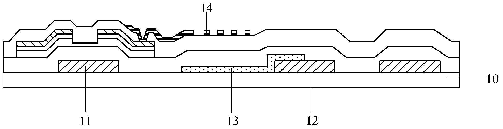
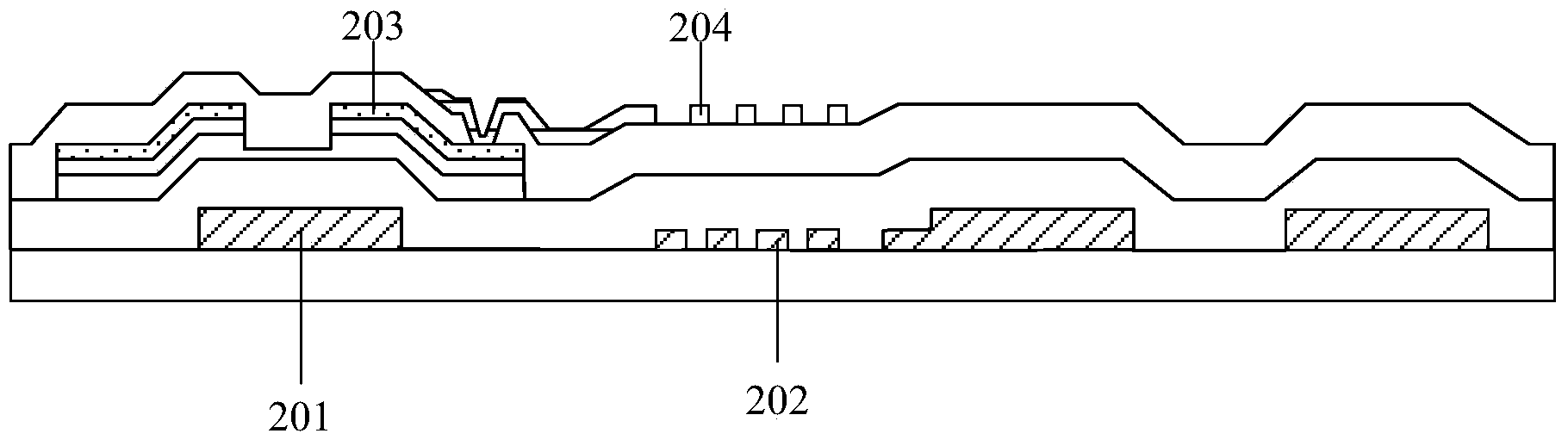
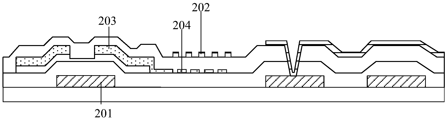
[0040] Embodiments of the present invention provide an array substrate, a display device, and a method for manufacturing the array substrate. The material of the pixel electrode is the same as that of the source and drain electrodes, but the thickness is smaller than that of the source and drain electrodes, or the material of the common electrode is the same as that of the gate electrode, but the thickness is smaller than that of the gate electrode. The thickness of the array substrate ensures the transmittance of the array substrate on the basis of reducing the difficulty of the process.

[0041] like Figure 2a or Figure 2b As shown, the array substrate provided by the embodiment of the present invention includes:

[0042] The gate electrode 201 and the common electrode 202 arranged on the same layer, or the source and drain electrodes 203 and the pixel electrode 204 arranged on the same layer, wherein,

[0043] When the grid 201 and the common electrode 202 are arranged ...


PUM


Abstract

The invention discloses an array substrate, a display device and an array substrate manufacturing method, and relates to the liquid crystal display technology. Material of a pixel electrode is the same as that of a source and drain electrode, but the thickness of the pixel electrode is smaller than that of the source and drain electrode, and alternatively material of a public electrode is the same as that of a grid electrode but the thickness of the public electrode is smaller than that of the grid electrode. On the basis of reducing technology difficulty, the transmittance of the array substrate is guaranteed.

Description

technical field [0001] The invention relates to liquid crystal display technology, in particular to an array substrate, a display device and a manufacturing method of the array substrate. Background technique [0002] Thin Film Transistor Liquid Crystal Display (TFT-LCD for short) has the characteristics of small size, low power consumption, and no radiation, and occupies a dominant position in the current flat panel display market. Advanced Super Dimension Switch technology (ADvanced Super Dimension Switch, referred to as ADS) generates a fringe electric field through the electrodes between pixels in the same plane, so that the aligned liquid crystal molecules between the electrodes and directly above the electrodes can be rotated in the direction of the plane (parallel to the substrate). , improve the light transmission efficiency of the liquid crystal layer while increasing the viewing angle. [0003] figure 1 It is a structural schematic diagram of the current ADS mode...

Claims


Application Information

Patent Timeline
Patent Type & Authority Applications(China)
IPC IPC(8): H01L27/12H01L21/77G02F1/1362G02F1/1368G02F1/1343
CPCH01L27/124H01L27/1288G02F1/134363G02F1/13439G02F1/1368G02F1/134372H01L21/283H01L29/45
Inventor 张锋曹占锋姚琪谷敬霞
Owner BOE TECH GRP CO LTD
Why Eureka
Try Eureka