Suspended nitride film LED device and manufacturing method

A technology for LED devices and nitrides, applied in semiconductor devices, electrical components, circuits, etc., can solve problems such as silicon substrate peeling, and achieve the effects of reducing internal loss, improving light extraction efficiency, and improving working life.

Active Publication Date: 2014-05-07
NANJING UNIV OF POSTS & TELECOMM
View PDF5 Cites 25 Cited by
  • Summary
  • Abstract
  • Description
  • Claims
  • Application Information

AI Technical Summary

Problems solved by technology

However, due to the absorption of blue light by silicon materi

Method used


Image

  • Suspended nitride film LED device and manufacturing method
  • Suspended nitride film LED device and manufacturing method
  • Suspended nitride film LED device and manufacturing method

Examples


Embodiment Construction

[0027] The present invention will be further described in detail below in conjunction with the accompanying drawings and specific embodiments.

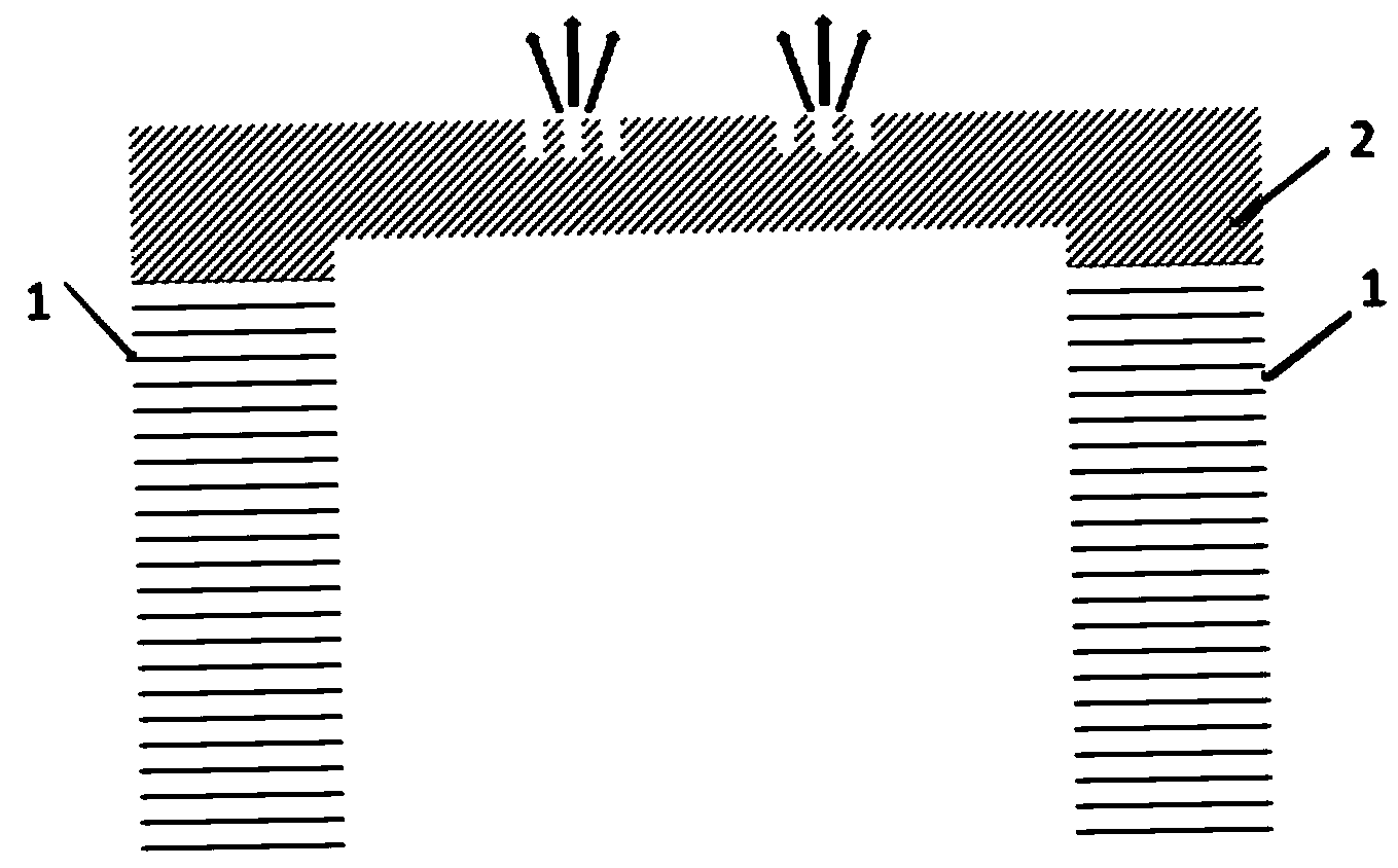
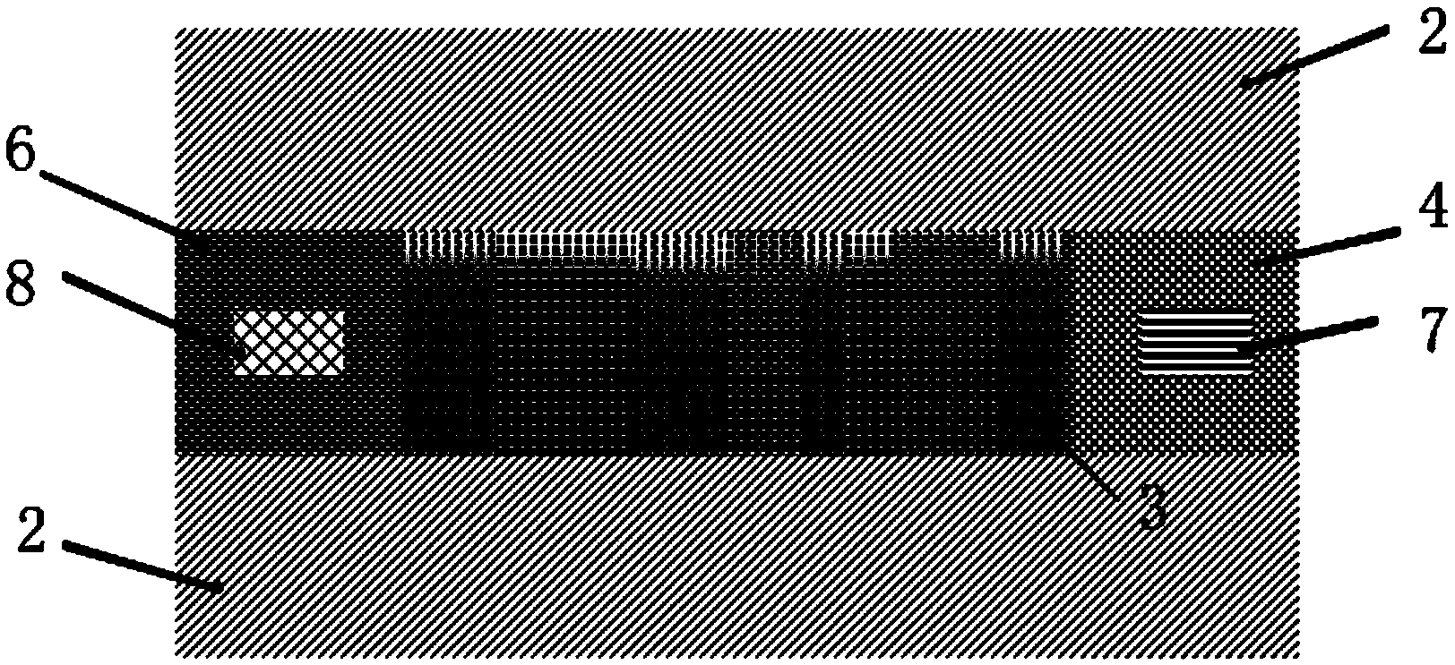
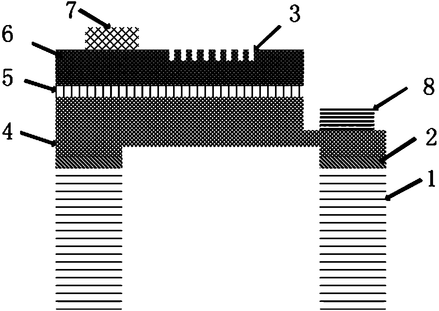
[0028] figure 1 , figure 2 , image 3 A schematic structural diagram of the suspended nitride thin film LED device of the present invention is given. The device uses a silicon-based nitride wafer with a P-N junction as a carrier, and includes a silicon substrate layer 1 and a gallium nitride layer disposed on the silicon substrate layer 1. 2. The P-N junction grown on the gallium nitride layer 2 and the resonant grating 3 arranged on the upper side of the P-N junction, the P-N junction and the resonant grating 3 constitute an LED light-emitting device, and the underside of the LED light-emitting device is provided with a penetrating silicon substrate layer 1 and as a buffer The cavity of the GaN layer 2 is used to make the LED light-emitting device completely suspended;

[0029] The P-N junction includes an N-GaN contact layer 4, ...


PUM


Abstract

The invention discloses a suspended nitride film LED device and a manufacturing method thereof. A carrier can be a silicon substrate nitride wafer. The suspended nitride film LED device comprises a top nitride device layer and a silicon substrate layer. The method can achieve stripping of high-refractive-index silicon substrate layer and the nitride device layer, eliminate absorption of exciting light by the silicon substrate layer, and achieve manufacturing of the suspended nitride film LED device. A nanostructure is arranged on the upper surface of the top nitride device layer and used for improving the interface state of nitrides and improving the light emitting efficiency. With the back aligning and deep silicon etching technology, the silicon substrate layer under the LED device is removed, and the suspended nitride film LED device is obtained; the nitride back thinning etching technology is further adopted to obtain the ultrathin suspended nitride film LED device, internal loss of the LED device is lowered, and the light emitting efficiency is improved.

Description

technical field [0001] The invention belongs to the technical field of information materials and devices, and relates to a suspended nitride thin film LED device and a preparation method thereof. Background technique [0002] With the breakthrough of nitride material growth technology, silicon substrate nitride wafers have gradually achieved technological breakthroughs and entered the commercial market. The development of silicon substrate nitride LED devices has broad application space. [0003] The gallium nitride LED in the past is grown on the sapphire substrate, but the gallium nitride LED of the present invention is grown on the silicon substrate. And combined with optical microelectromechanical devices (MEMS). Realize the control of light waves, and improve the efficiency of light output at the same time. There is a nanostructure on the upper surface of the nitride device layer, which is a resonant grating, which is used to improve the interface state of the nitrid...

Claims


Application Information

Patent Timeline
IPC IPC(8): H01L33/00H01L33/06H01L33/32H01L33/22
CPCH01L33/0066H01L33/0075H01L33/0093H01L33/06H01L33/20H01L33/32
Inventor 王永进白丹施政李欣高绪敏陈佳佳朱洪波
Owner NANJING UNIV OF POSTS & TELECOMM
Why Eureka
Try Eureka