

Flyback converter and power supply system
A flyback converter and circuit technology, applied in control/regulation systems, instruments, DC power input conversion to DC power output, etc., to achieve the effects of reducing difficulty, suppressing output cross-adjustment, and facilitating matching
- Summary
- Abstract
- Description
- Claims
- Application Information
AI Technical Summary
Problems solved by technology
Method used
Image

Examples
Embodiment 1
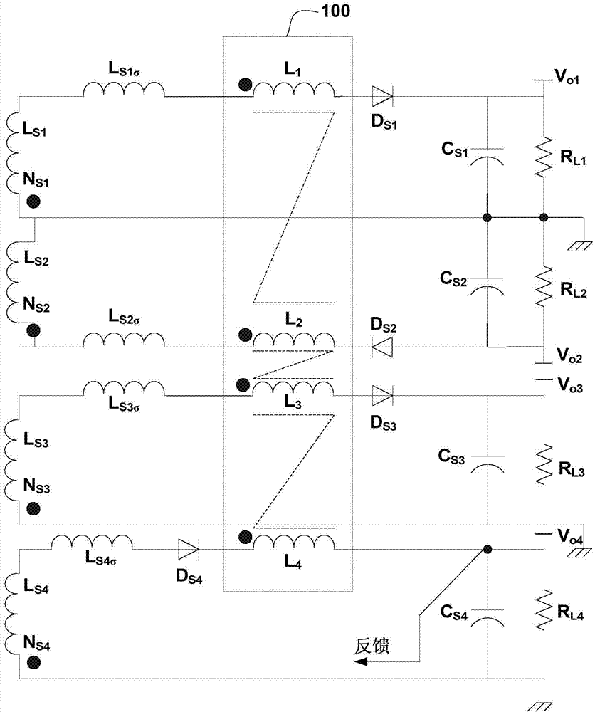
[0026] figure 1 The circuit diagram of the flyback converter secondary circuit provided for Embodiment 1 of the present invention, such as figure 1 As shown, the flyback converter includes a primary circuit and a secondary circuit, wherein the secondary circuit includes four output circuits, and each output circuit includes a first secondary winding N S , the second secondary winding L S , Secondary winding output leakage inductance L Sσ , series inductor L, rectifier tube D S , output capacitance C S and the resistor R L .
[0027] Taking the first output circuit as an example, the first secondary winding N in the first S1 , the second secondary winding L S1 , Secondary winding output leakage inductance L S1σ , series inductance L 1 , rectifier tube D S1 with output capacitor C S1 series, the output capacitor C S1 with the resistor R L1 in parallel, the resistor R L1 Connect one end to the output voltage V o1 , the resistor R L1 The other end is grounded. The...
Embodiment 2
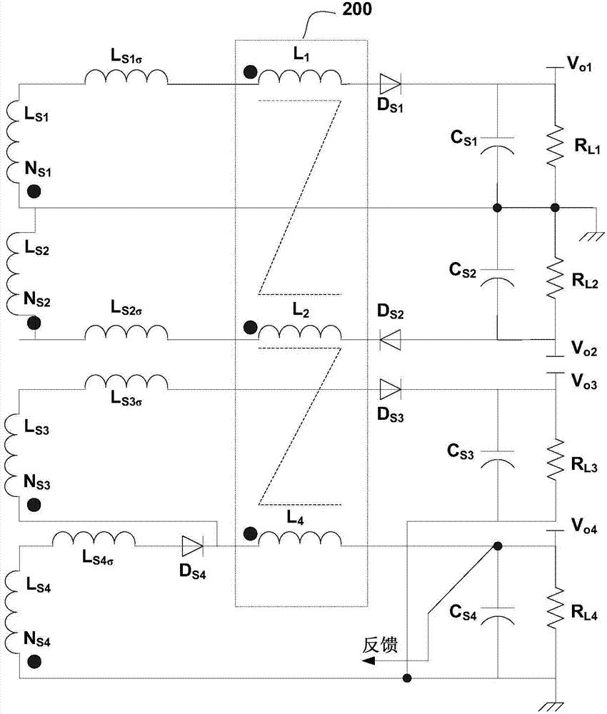
[0030] figure 2 The circuit diagram of the secondary circuit of the flyback converter provided by Embodiment 2 of the present invention. The secondary circuit of the flyback converter provided in this embodiment is based on the previous embodiment. If there are two output circuits with output voltage V o Common ground, and the output voltage V of the first output circuit in the two output circuits o higher than the output voltage V of the second output circuit o , then the first secondary winding N of the first output circuit S The negative terminal is connected to the rectifier tube D of the second output circuit S The cathode of the DC superposition technique can be used to save the series inductance L of the first output circuit.
[0031] The following takes the third output circuit and the fourth output circuit as examples for explanation, as shown in figure 2 As shown, the output voltage V of the third output circuit o3 and the output voltage V of the fourth output...
Embodiment 3
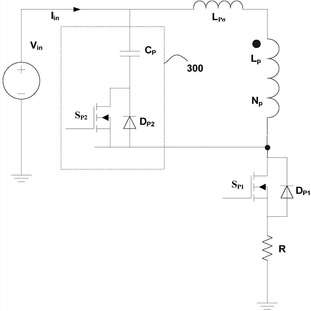
[0034] image 3 The circuit diagram of the primary side circuit of the flyback converter provided by Embodiment 3 of the present invention. The flyback converter of this embodiment is based on Embodiment 1 or Embodiment 2. The primary side circuit is an active clamping circuit, including Primary winding N P , Primary inductance L P , Primary leakage inductance L Pσ , switch tube (S P1 , S P2 ), capacitance C P , rectifier tube (D P1 、D P2 ) and resistor R, the switch S P2 with rectifier D P2 After parallel connection with capacitor C P connected in series to form an active clamp circuit 300, the primary winding N P , Primary inductance L P and the primary side leakage inductance L Pσ After being connected in series with the active clamp circuit 300 in parallel, one end is connected to the input voltage V in , one end is in turn connected with the switch tube S P1 with rectifier D P1 The parallel circuit and the resistor R are connected in series.
[0035] ima...
PUM
 Abstract
Description
Claims
Application Information