InGaAs infrared photodetector

A detector and infrared light technology, which is applied in semiconductor devices, electrical components, circuits, etc., can solve the problems of light absorption reduction and quantum efficiency reduction, so as to achieve the advantages of thinning the absorption layer, reducing dark current, and compensating for low quantum efficiency. Effect

Active Publication Date: 2014-05-21
河北光森电子科技有限公司
View PDF3 Cites 13 Cited by
  • Summary
  • Abstract
  • Description
  • Claims
  • Application Information

AI Technical Summary

Problems solved by technology

[0005] In the process of realizing the present invention, the applicant found that the existing use of a thin layer of InGaAs material as the absorption region can reduce th

Method used


Image

  • InGaAs infrared photodetector
  • InGaAs infrared photodetector
  • InGaAs infrared photodetector

Examples


Embodiment Construction

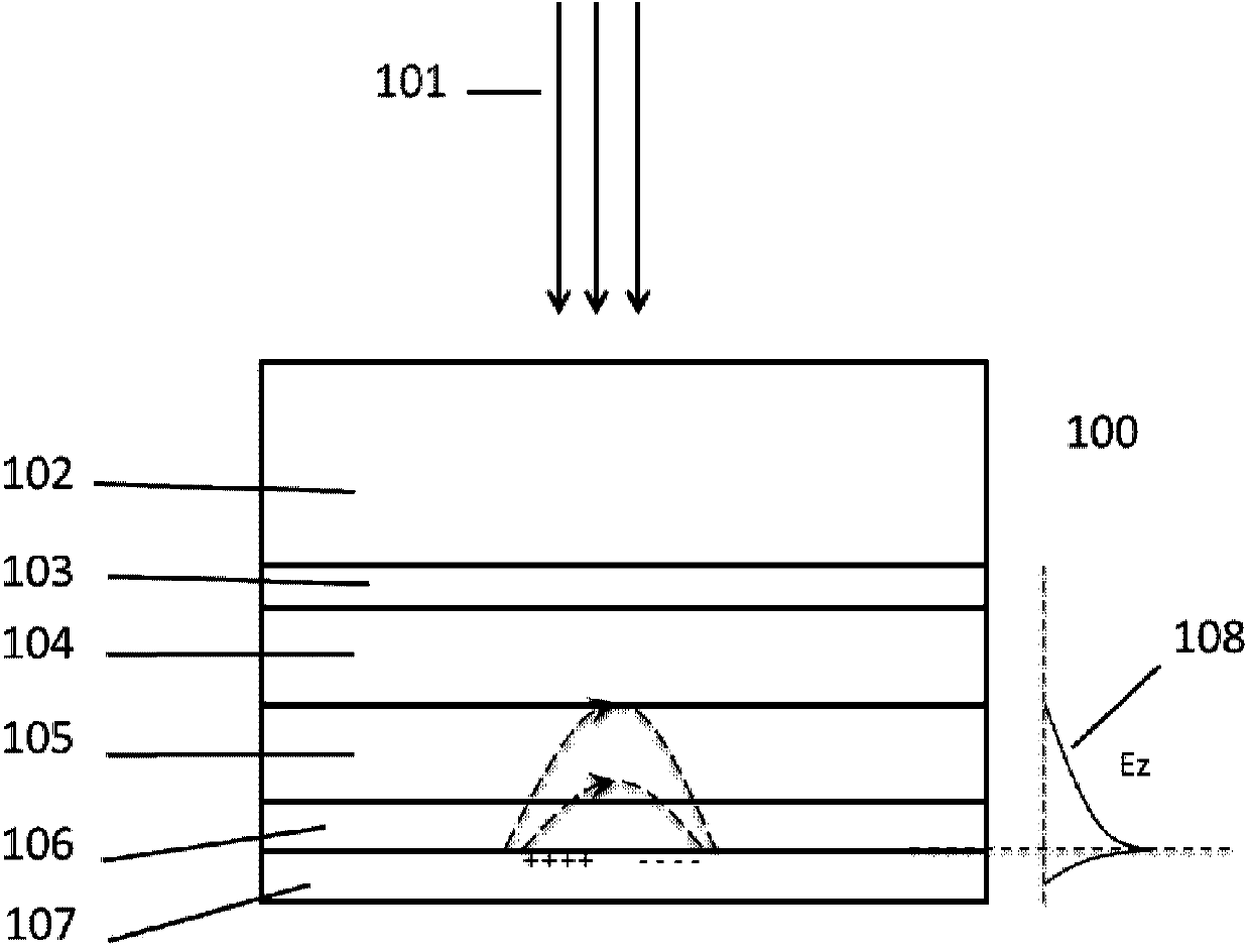
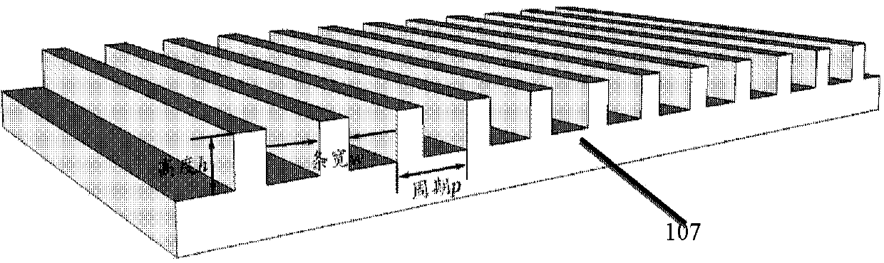
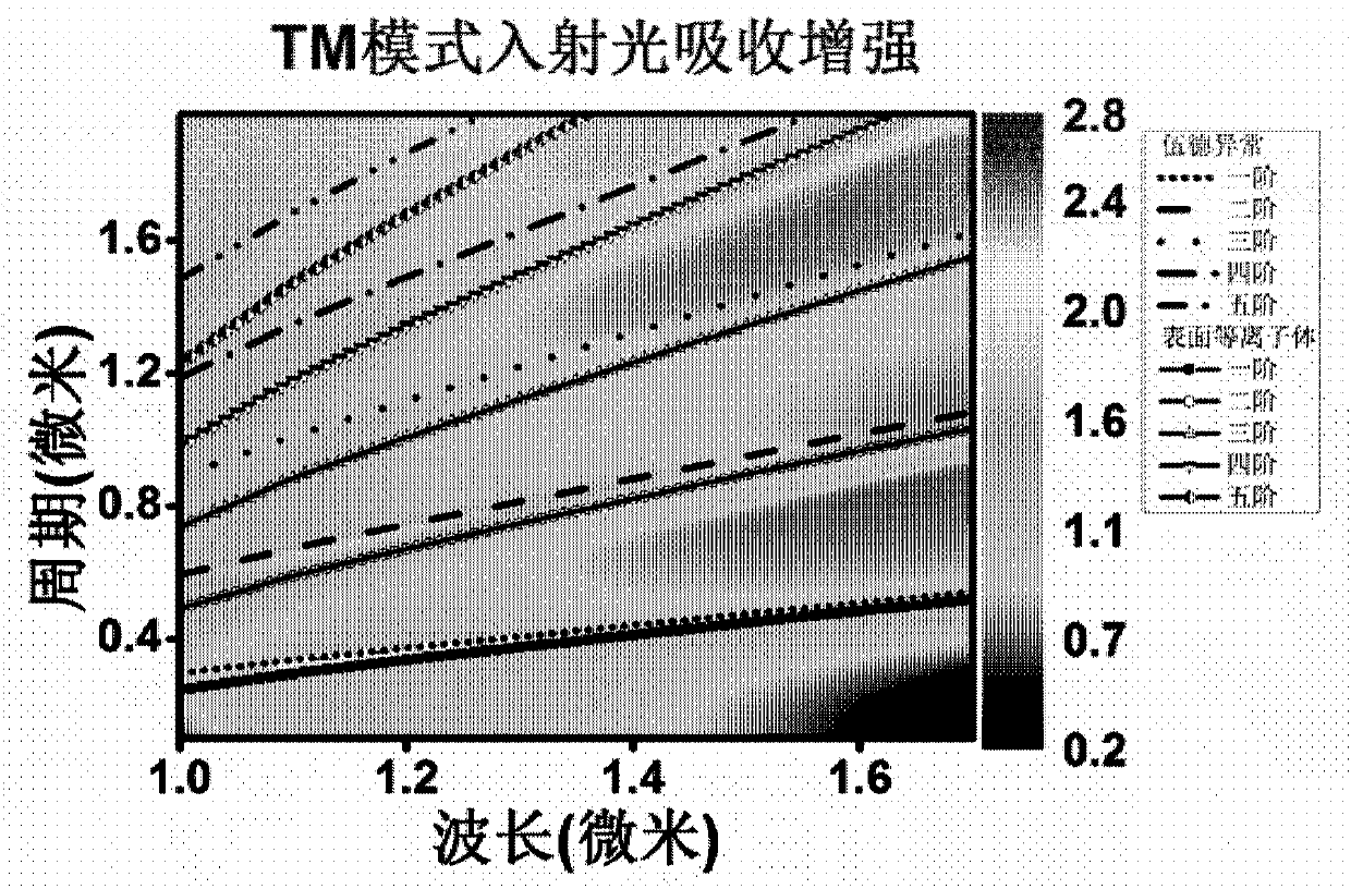
[0024] In order to make the object, technical solution and advantages of the present invention clearer, the present invention will be described in further detail below in conjunction with specific embodiments and with reference to the accompanying drawings. It should be noted that, in the drawings or descriptions of the specification, similar or identical parts all use the same figure numbers. Implementations not shown or described in the accompanying drawings are forms known to those of ordinary skill in the art. Additionally, while illustrations of parameters including particular values ​​may be provided herein, it should be understood that the parameters need not be exactly equal to the corresponding values, but rather may approximate the corresponding values ​​within acceptable error margins or design constraints. The directional terms mentioned in the embodiments, such as "upper", "lower", "front", "rear", "left", "right", etc., are only referring to the directions of the...


PUM

PropertyMeasurementUnit
Thicknessaaaaaaaaaa
Heightaaaaaaaaaa
Thicknessaaaaaaaaaa

Abstract

The invention provides an InGaAs infrared photodetector. The InGaAs infrared photodetector comprises a semiconductor substrate of which both faces are polished, and a lower doped layer, an absorption layer, an upper doped layer and a metal grating layer deposited in sequence on the semiconductor substrate, wherein the absorption layer is an intrinsically-doped or low-concentration-doped InGaAs material; the metal grating layer is a one-dimensional periodic sub-wavelength grating; the lower doped layer and the upper doped layer are heavily-doped InGaAs materials of different doping types, and construct a pin structure with the absorption layer respectively; the two electrodes of the InGaAs infrared photodetector are electrically connected to the lower doped layer and the upper doped layer respectively, and are used for introducing external bias voltage and collecting detection signals. According to the InGaAs infrared photodetector, a surface plasma effect and a Rayleigh-Wood abnormity effect are excited by using a one-dimensional periodic metal grating, thereby increasing the response speed of a device under the condition of not losing the absorptivity.

Description

technical field [0001] The invention relates to the technical field of photodetectors, in particular to an InGaAs infrared photodetector. Background technique [0002] Infrared detectors are the core components of infrared systems and thermal imaging systems, and InGaAs material is an excellent near-infrared photoelectric detection material. In the field of near-infrared detection, the material systems that can be applied in the 1 μm ~ 3 μm band are mainly based on mercury cadmium telluride (HgCdTe), indium antimonide (InSb) and indium gallium arsenide (InGaAs). [0003] HgCdTe detectors can work in the 1μm~3μm band through energy band clipping. Affected by the background limitation, the refrigeration temperature is usually required to be below 150K. The weak Te-Hg bond in this material system will bring a series of problems, such as material Large-area uniformity problems, process stability, and space application radiation problems; InSb detectors cover wavelengths in the ...

Claims


Application Information

Patent Timeline
IPC IPC(8): H01L31/105H01L31/0232
CPCH01L31/02327H01L31/1035H01L31/1844
Inventor 韦欣许斌宗宋国峰刘杰涛徐云相春平付东
Owner 河北光森电子科技有限公司
Why Eureka
Try Eureka