

Semiconductor device and manufacturing method of the same
A technology for semiconductors and devices, which is applied in the field of semiconductor devices with planarization films and its manufacturing, and can solve problems such as cracks in semiconductor chips
- Summary
- Abstract
- Description
- Claims
- Application Information
AI Technical Summary
Problems solved by technology
Method used
Image

Examples
no. 1 example
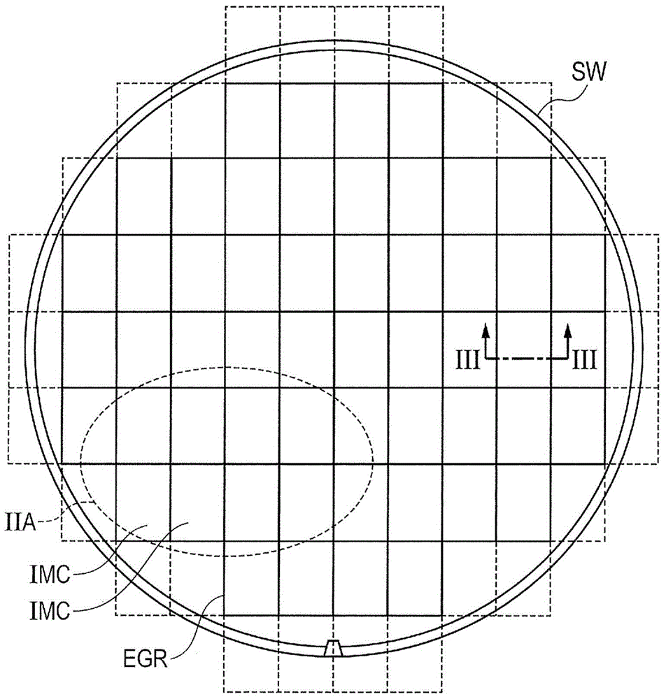
[0056] now refer to figure 1 , a semiconductor device in a wafer state will be described as an example.
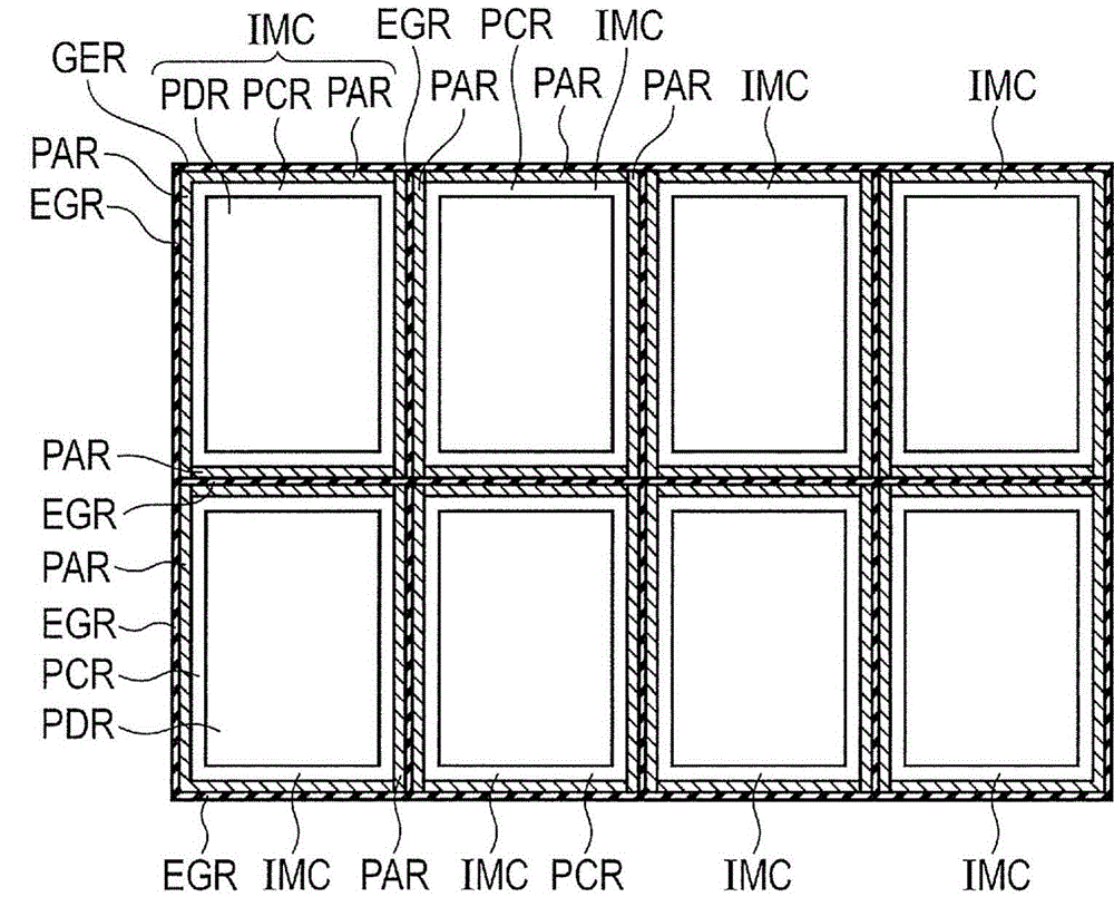
[0057] refer to figure 1 , the semiconductor wafer SW is composed of silicon single crystal, for example. A plurality of chip regions IMC for image sensors are arranged on the main surface of the semiconductor wafer SW. Each chip region IMC for an image sensor has a rectangular planar shape, and they are arranged in a matrix pattern. A region between a pair of adjacent chip regions IMC on the main surface of the semiconductor wafer SW is an edge region EGR (non-element region). The edge region EGR has a rectangular shape surrounding the periphery of the chip region IMC, and isolates each of the plurality of chip regions IMC on the main surface of the semiconductor wafer SW. Moreover, in figure 1 Near the periphery of the semiconductor wafer SW, in the area surrounded by the dotted line and the edge region EGR, a part of the rectangle which is the chip region is cut of...
no. 2 example
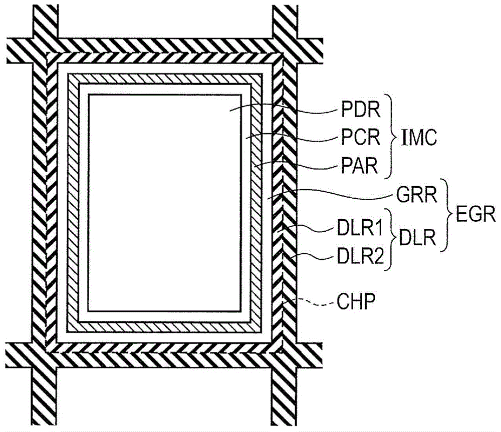
[0125] refer to Figure 9 , the configuration of each part of the semiconductor chip CHP of the present embodiment will be described.
[0126] refer to Figure 9 , the semiconductor chip CHP of this embodiment has the same characteristics as the semiconductor chip CHP of the first embodiment ( image 3 ) basically the same configuration. However, the semiconductor chip CHP of the present embodiment is different from the first embodiment in that the first slot SLT1 is formed in the edge region EGR.
[0127] The first slot SLT1 is formed in the level difference LVL which is a removed portion of the passivation film PAS. More specifically, the first slot SLT1 is formed in a part region of the upper surface of the planarizing film FF that is the bottom surface of the level difference LVL as a region (removed portion) in which the planarizing film FF is removed. The first slot SLT1 is formed right above the top-layer metal wiring TML of the guard ring GR. Also, the first slot ...
no. 3 example
[0141] First, refer to Figure 13 , the configuration of each part of the semiconductor chip CHP of the present embodiment will be described.
[0142] refer to Figure 13 , the semiconductor chip CHP of this embodiment has the same characteristics as the semiconductor chip CHP of the first and second embodiments ( image 3 and 9 ) basically the same configuration. However, in the case of the semiconductor chip CHP according to the present embodiment, in plan view, outside the top metal wiring TML of the guard ring GR (on the other side with respect to the top metal wiring TML of the photodiode region PDR: Figure 13 The right side in ) forms the first slot SLT1 in the level difference LVL of the edge region EGR. Specifically, the first slot SLT1 is formed, for example, in the scribe region DLR.
[0143] Figure 13 The first slot SLT1 in is formed in a part of the region of the upper surface of the planarizing film FF that is the bottom surface of the level difference LVL...
PUM
| Property | Measurement | Unit |
|---|---|---|
| Film thickness | aaaaa | aaaaa |
Abstract
Description
Claims
Application Information