Method for manufacturing double-layer graphene electrooptical modulator on basis of silicon substrate optical waveguide micro-ring resonant cavity

A micro-ring resonator, double-layer graphene technology, applied in the field of integrated optics, can solve the problems of increasing insertion loss, increasing process difficulty, etc., and achieve the effects of enhancing modulation strength, avoiding insertion loss, and small structure size

Inactive Publication Date: 2014-06-18
ZHONGBEI UNIV
View PDF4 Cites 15 Cited by
  • Summary
  • Abstract
  • Description
  • Claims
  • Application Information

AI Technical Summary

Problems solved by technology

However, since this single-layer graphene structure needs to dope the underlying silico...

Method used


Image

  • Method for manufacturing double-layer graphene electrooptical modulator on basis of silicon substrate optical waveguide micro-ring resonant cavity
  • Method for manufacturing double-layer graphene electrooptical modulator on basis of silicon substrate optical waveguide micro-ring resonant cavity
  • Method for manufacturing double-layer graphene electrooptical modulator on basis of silicon substrate optical waveguide micro-ring resonant cavity

Examples


Embodiment Construction

[0021] The present invention will be further described below in conjunction with accompanying drawing:

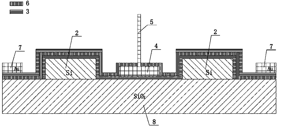
[0022] Such as figure 1 , 2 As shown, a method for preparing a double-layer graphene electro-optic modulator based on a silicon-based optical waveguide microring resonator comprises the following steps:

[0023] 1) Simulation and design of optical waveguide microring resonator

[0024] Use Optiwave-FDTD and Rsoft to simulate and analyze SOI-based micro-ring cavities with different parameters, screen out designs with higher Q values, and then prepare L-edit layouts for process tape-out;

[0025] 2) Process preparation of optical waveguide microring resonator

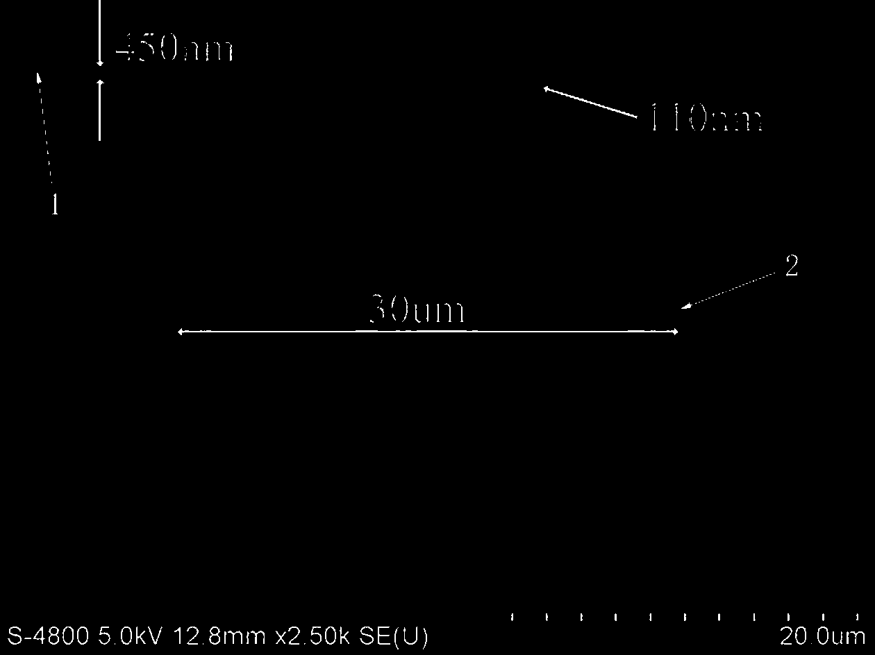
[0026] Take the existing SOI sheet, the silicon on the top layer of the existing SOI sheet is 220nm, and the thickness of the oxide layer is 3um. The SOI sheet is processed by electron beam lithography, ICP etching, and high temperature annealing process and the surface is smooth. Chemical treatment, the w...


PUM


Abstract

The invention provides a method for manufacturing a double-layer graphene electrooptical modulator on the basis of a silicon substrate optical waveguide micro-ring resonant cavity. The method comprises the steps that firstly, simulation and design of the silicon substrate optical waveguide micro-ring resonant cavity are conducted, and the design with a high Q value is selected, process tape-out is conducted; secondly, an existing SOI piece is taken out for process preparation of the silicon substrate optical waveguide micro-ring resonant cavity, and two layers of graphene and one layer of AL2O3 grow on the prepared silicon substrate optical waveguide micro-ring resonant cavity; finally, two electrodes which are symmetrically distributed are led. The method can provide very strong interaction of graphene and light and high-strength photovoltaic conversion. As light absorption of the graphene is unrelated to the light wavelength, broadband control can be conducted; meanwhile, carrier mobility of the graphene at room temperature is extremely high, and modulation time can be reduced to the picosecond level by exerting an external electric field; in addition, the method and a CMOS process can be compatible, and therefore the method is greatly meaningful to microminiaturization, high speed and low power consumption of later integrated optics chips.

Description

technical field [0001] The invention belongs to the technical field of integrated optics, in particular to a method for preparing a double-layer graphene electro-optic modulator based on a silicon-based optical waveguide microring resonator cavity. Background technique [0002] The modulator is one of the key components of optical communication. A lot of research work has been done on the modulator at home and abroad. Up to now, its basic performance such as modulation speed, bandwidth and integration density has been greatly improved. However, the future optoelectronic interconnection It is required to have higher performance, so the modulator has always been a research hotspot. Silicon-based optical waveguide optical modulators have attracted the attention of many researchers at home and abroad because of their ease of integration. In recent years, research on integrated optical waveguide optical modulators has gradually become a hot spot, and many related achievements an...

Claims


Application Information

Patent Timeline
IPC IPC(8): G02F1/035
Inventor 张文栋薛晨阳王永华熊继军刘俊韦丽萍崔丹凤王永存
Owner ZHONGBEI UNIV
Why Eureka
Try Eureka