Cascode circuit

A circuit and cascading technology, applied in circuits, electronic switches, electrical components, etc., to improve cost/performance and minimize internal inductance

Active Publication Date: 2014-06-18
NEXPERIA BV
View PDF3 Cites 17 Cited by
  • Summary
  • Abstract
  • Description
  • Claims
  • Application Information

AI Technical Summary

Problems solved by technology

[0020] Another problem with the basic cascode circuit described above (i.e., without additional components) is that it is designed as a three-terminal circuit to connect to the source, drain and gate terminals in an external circuit

Method used


Image

  • Cascode circuit
  • Cascode circuit
  • Cascode circuit

Examples


Embodiment Construction

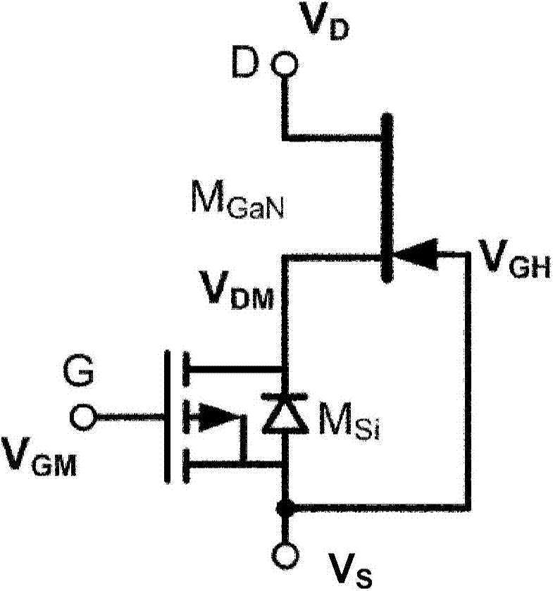
[0054] The present invention provides a cascode circuit structure in which low-voltage MOSFETs and depletion-mode power devices are mounted on a substrate (e.g., a ceramic substrate), which can then be provided in a semiconductor package (or sold separately to those wishing to customers who produce their own modules). Only GaN devices will be referred to below, but the same approach applies to SiC devices or other depletion mode devices. The present invention is concerned with high electron mobility transistors or junction gate field effect transistors.

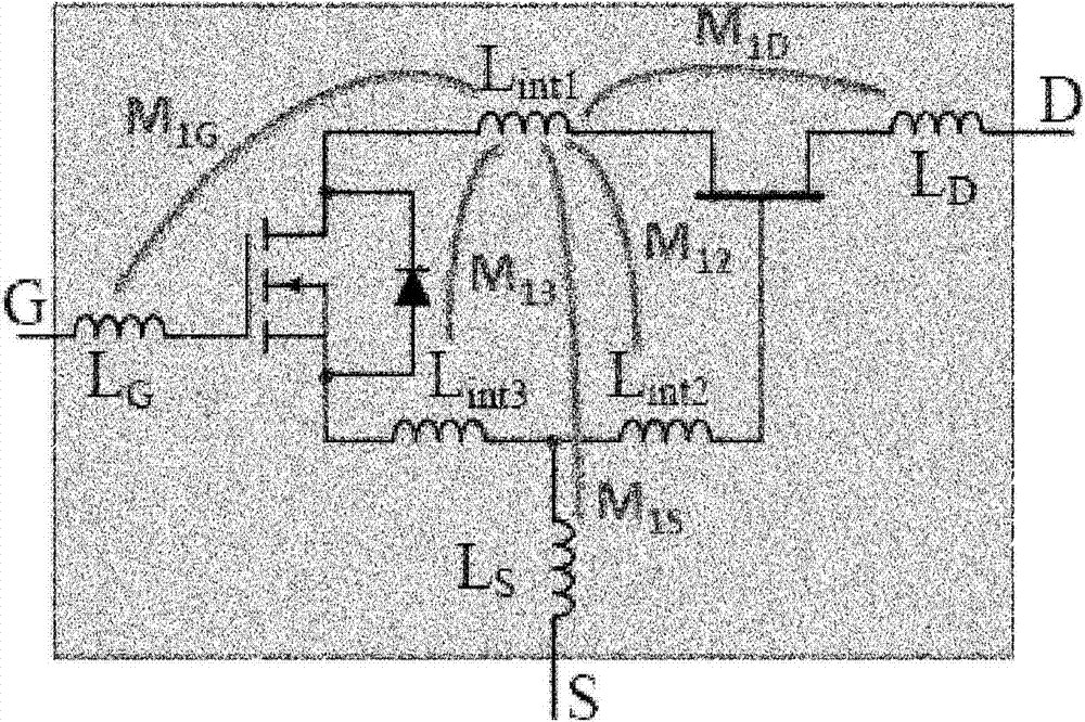
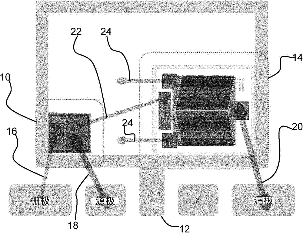
[0055] Figure 4 A circuit example of the present invention is shown. shows the layout of the components, but the circuit corresponds to figure 1 (although as noted below in Figure 4 optional additional components are shown).

[0056] The circuit has a first gallium nitride or silicon carbide field effect transistor 40 with a drain D for connection to the high power supply line. The drain of the second silicon MOSFET 4...


PUM


Abstract

A cascode circuit arrangement has a low voltage MOSFET and a depletion mode power device mounted on a substrate (for example a ceramic substrate), which can then be placed in a semiconductor package. This enables inductances to be reduced, and can enable a three terminal packages to be used if desired.

Description

technical field [0001] The present invention relates to cascaded semiconductor devices. In particular, the invention relates to depletion mode transistors, eg high electron mobility transistors or junction gate field effect transistors. Examples are gallium nitride (GaN) transistors (eg GaN high electron mobility transistors (HEMTs)) or silicon carbide (SiC) field effect transistors. Background technique [0002] The present invention is particularly concerned with GaN power transistors. The base GaN power semiconductor is a depletion mode (normally on) device due to the presence of built-in heterojunctions created during the growth of the GaN wafer. This creates thin regions of high conductivity in the material, called two-dimensional electron gas ("2DEG"), that effectively define the transistor channel. [0003] In order to make a normally-off GaN device, a means of disturbing the 2DEG to prevent it from being turned on is required. Attempts have been made to introduce...

Claims


Application Information

Patent Timeline
Patent Type & Authority Applications(China)
IPC IPC(8): H01L23/52H02M1/00
CPCH01L23/49575H01L23/49562H01L27/0629H01L2224/48257H01L2224/48247H03K17/567H01L23/4824H01L23/49531H01L25/072H01L2224/49171H01L2924/30107H01L2924/13091H01L2924/13055H01L2924/12032H01L2224/48137H01L2224/49175H01L2224/0603H01L2224/4903H01L2924/00
Inventor 菲利普·鲁特尔简·雄斯基马塞厄斯·罗斯
Owner NEXPERIA BV
Why Eureka
Try Eureka