Electric programmable fuse structure

A fuse structure and fuse technology, applied in circuits, electrical components, electrical solid devices, etc., can solve the problems of easy splashing of residues into surrounding circuits, reduced chip reliability, unfavorable device miniaturization, etc., to achieve enhanced electron migration Function, improvement of utilization rate, effect of breaking easily

Active Publication Date: 2014-06-18
SEMICON MFG INT (SHANGHAI) CORP
View PDF6 Cites 3 Cited by
  • Summary
  • Abstract
  • Description
  • Claims
  • Application Information

AI Technical Summary

Problems solved by technology

[0009] The problem solved by the present invention is that when the existing fuse structure breaks, the area of ​​the cathode area is too small, and the residue is easily splashed into the surrounding circuit, which reduces the reliability of the chip, and the area of ​​the cathode area is too large, which is not conducive to the miniaturization of the entire device. change

Method used


Image

  • Electric programmable fuse structure
  • Electric programmable fuse structure
  • Electric programmable fuse structure

Examples


Embodiment 1

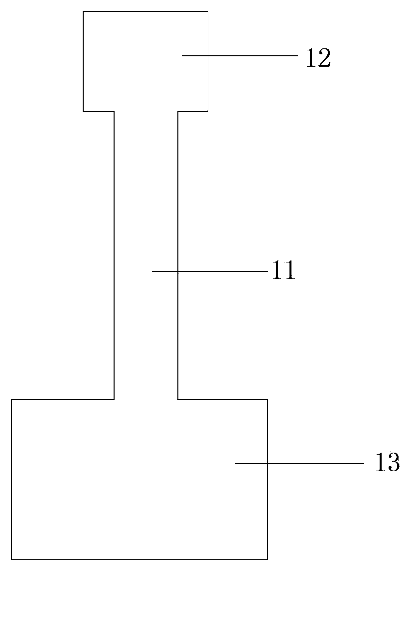
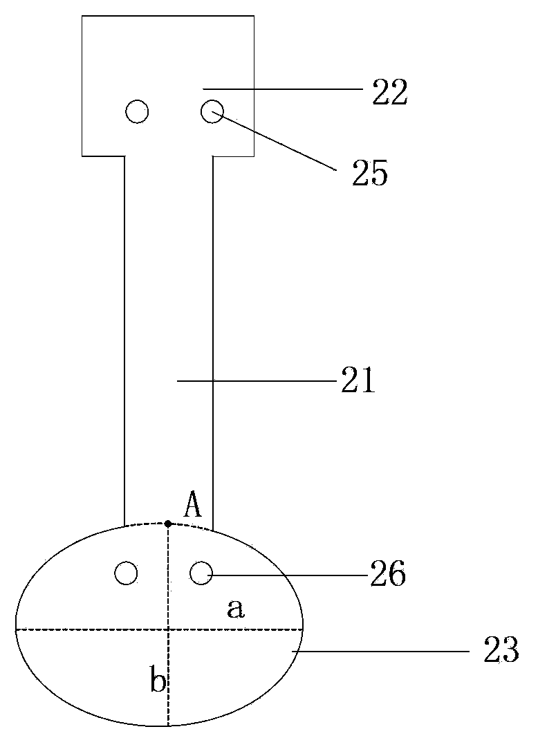
[0047] refer to image 3 As shown in the top view, the e-fuse structure includes:

[0048] an anode region 22, having a first contact window 25 thereon, and the first contact window 25 is suitable for coupling a high voltage during the programming process of the fuse structure;

[0049] a cathode region 23 having a second contact window 26 thereon, the second contact window 26 being suitable for coupling a low voltage during programming of the fuse structure;

[0050] A fuse connection area 21, one end of which is connected to the anode area 22, and the other end is connected to the cathode area 23;

[0051] Wherein, the cathode region 23 is in the shape of an ellipse, and the fuse connection region 21 is connected to the endpoint A of the minor axis of the ellipse.

[0052] The first contact window 25 and the second contact window 26 may be contact holes or metal interconnection structures, and this embodiment takes contact holes as an example.

[0053] The materials of th...

Embodiment 2

[0059] The structure of the e-fuse provided in the second embodiment is substantially the same as that in the first embodiment. The difference is that in order to enhance the probability of breaking the fuse link region 21 in the section close to the cathode region 23 , the ability of the cathode region 23 to transport electrons is improved. In other words, the ability of the cathode region 23 to transport electrons is stronger than that of the anode region 22 .

[0060] Specifically, in the semiconductor process, based on repeatability considerations, the second contact window 26 located in the cathode region 23 has the same shape as the first contact window 25 located in the anode region 22 (for example, when it is a conductive plug, the shape of the conductive plug same diameter), that is, when the number of contact windows 25, 26 located in each polar region 22, 23 is the same, the ability of each polar region 22, 23 to transport electrons is the same. In order to improve ...
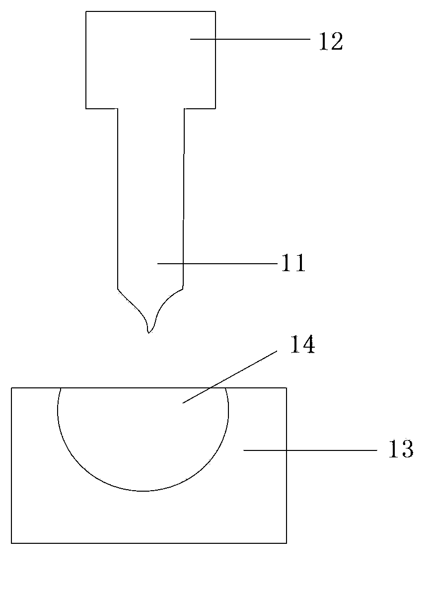
Embodiment 3

[0063] The structure of the e-fuse provided in the third embodiment is roughly the same as that in the first and second embodiments. The difference is that, in order to make the fuse link region 21 easier to break, as Figure 7 As shown, a PN junction is formed in the polysilicon layer 20, and when a high voltage is applied to the anode region 22, the PN junction is reverse-biased. Due to the existence of the reverse-biased PN junction, no large programming current passes through the polysilicon layer 20, and a large programming current Passing through the fuse link area 21 is easier to break.

[0064] Correspondingly, the polysilicon layer 20 below the anode region 22 is correspondingly doped with N-type ions, such as P, As. The polysilicon layer 20 below the cathode region 23 is correspondingly doped with P-type ions, such as B.


PUM


Abstract

The invention provides an electric programmable fuse structure. According to the electric programmable fuse structure provided by the invention, an elliptical cathode region, which is different from a rectangular or square cathode region generally adopted by the prior art, is adopted by the electric programmable fuse structure, a fuse connecting region is connected to an elliptical short shaft end point, thus the situation that bursting residue is borne to the maximum by adopting smaller cathode region area is realized, the residue is not easy to splash into a surrounding circuit, and the electric programmable fuse structure is beneficial for device miniaturization as the area is smaller.

Description

technical field [0001] The invention relates to the field of semiconductor manufacturing, in particular to an electric programmable fuse structure. Background technique [0002] As the miniaturization and complexity of semiconductor devices increase, the degree to which these devices are adversely affected by various defects or impurities also increases. For example, the failure of a single metal connection, diode or transistor often leads to a decrease in the yield of the entire chip. In view of the above problems, the prior art proposes to form some spare units in the integrated circuit to repair or replace the defect area, which is called redundancy technology (Redundancy technology). The above-mentioned backup unit is connected to the main device through some fusible links (fusible links), that is, fuses (fuse). The selective connection of the fuses provides the possibility to modify the circuit after the chip has been fabricated. [0003] Existing fuses are roughly di...

Claims


Application Information

Patent Timeline
Patent Type & Authority Applications(China)
IPC IPC(8): H01L23/525
Inventor 张海洋李天慧舒强
Owner SEMICON MFG INT (SHANGHAI) CORP
Why Eureka
Try Eureka