Epitaxial wafer structure and epitaxial wafer surface roughening method

A surface roughening and epitaxial wafer technology, which is applied to semiconductor devices, electrical components, circuits, etc., can solve the problems of no contribution to light emission, rising LED chip temperature, and high production costs, so as to improve light extraction efficiency and strong operability , The effect of simple process

Active Publication Date: 2014-06-25
BYD SEMICON CO LTD
View PDF6 Cites 0 Cited by
  • Summary
  • Abstract
  • Description
  • Claims
  • Application Information

AI Technical Summary

Problems solved by technology

With such a large difference in refractive index, a large amount of light is reflected back during the propagation of light from an optically denser medium to an optically thinner medium, and finally disappears in the LED chip in the form of heat, which does not contribute to the luminescence of the LED, but instead causes the LED The internal temperature of the chip rises, which affects the life and luminous efficiency of the LED
[0003] Now, there is a way to improve the light output by roughening the surface of the LED chip, which is mainly to roughen the contact surface between the optically dense medium and the optically sparse medium, and to improve the light output efficiency of the LED chip by changing the incident angle. Usually, ICP is used. Bombarding the surface of the LED to achieve the purpose of roughening, which requires relatively expensive ICP etching equipment, and the production cost is relatively high

Method used


Image

  • Epitaxial wafer structure and epitaxial wafer surface roughening method
  • Epitaxial wafer structure and epitaxial wafer surface roughening method

Examples


Embodiment Construction

[0017] In order to make the technical problems, technical solutions and beneficial effects solved by the present invention clearer, the present invention will be further described in detail below in conjunction with the embodiments. It should be understood that the specific embodiments described here are only used to explain the present invention, not to limit the present invention.

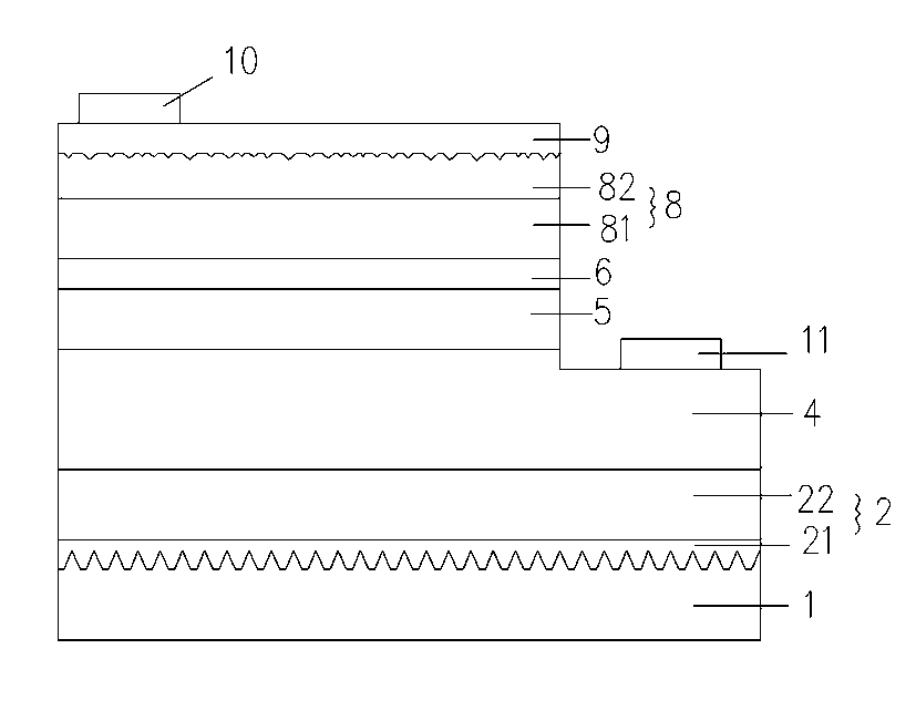
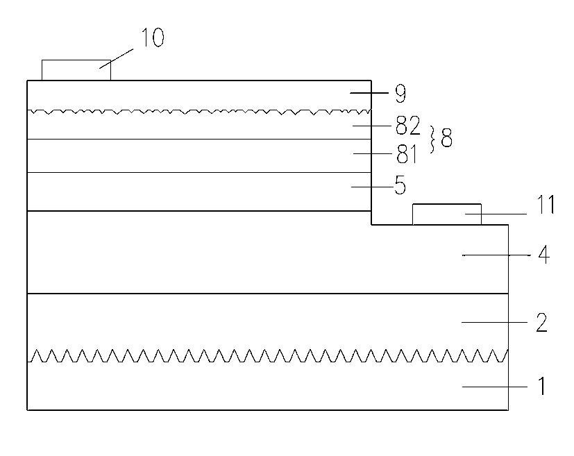
[0018] Such as figure 1 and figure 2 As shown, the present invention provides an epitaxial wafer structure, including a substrate 1, and a buffer layer 2, a first-type nitride layer 4, a light-emitting layer 5, and a second-type nitride layer 8 sequentially formed on the substrate 1, The second type nitride layer 8 includes a first nitride layer 81 and a second nitride layer 82 sequentially formed on the light emitting layer, the second nitride layer 82 is a heavily doped nitride layer, the Pits are distributed on the surface of the second nitride layer 82 .

[0019] In the present invention,...


PUM

PropertyMeasurementUnit
Doping concentrationaaaaaaaaaa
Thicknessaaaaaaaaaa
Depthaaaaaaaaaa

Abstract

The invention provides an epitaxial wafer structure comprising a substrate, a buffer layer, a first type nitride layer, a luminescent layer and a second type nitride layer. The buffer layer, the first type nitride layer, the luminescent layer and the second type nitride layer are successively formed on the substrate. The second type nitride layer includes a first nitride layer and a second nitride layer, wherein the first nitride layer and the second nitride layer are successively formed on the luminescent layer; the second nitride layer is a heavy-doping nitride layer; and pits are distributed on the surface of the second nitride layer. According to the invention, the heavy-doping nitride layer is added on the epitaxial wafer and chemical corrosion is carried out on the surface of the heavy-doping nitride layer. Because the doped impurity concentration of the heavy-doping nitride layer is high and defects are easily formed and thus the corrosion speed at the defected places is fast, thereby forming pits at the surface of the epitaxial wafer and achieving an objective of epitaxial wafer surface roughening. Therefore, the luminous efficiency of the epitaxial wafer can be effectively improved.

Description

technical field [0001] The invention belongs to the field of semiconductors, in particular to a method for roughening an epitaxial wafer. Background technique [0002] Light-emitting diode (LED) is a junction-type electroluminescent semiconductor device that can convert electrical signals into optical signals. Due to the large refractive index difference between the material used to make LEDs and the outside air, for example, blue light, green light and white light are currently produced. The main material of LED is III-V gallium nitride. The refractive index of gallium nitride material is about 2.5, while the refractive index of external air is 1. With such a large difference in refractive index, a large amount of light is reflected back during the propagation of light from an optically denser medium to an optically thinner medium, and finally disappears in the LED chip in the form of heat, which does not contribute to the luminescence of the LED, but instead causes the LED...

Claims


Application Information

Patent Timeline
IPC IPC(8): H01L33/22H01L33/00
CPCH01L33/007H01L33/0075H01L33/22
Inventor 谢春林
Owner BYD SEMICON CO LTD
Why Eureka
Try Eureka