A manufacturing process of a transparent substrate LED light bar

A technology of LED light strips and transparent substrates, applied to semiconductor devices, electrical components, circuits, etc., can solve the problems of multiple production processes, poor luminous effects, and increased production costs, and achieve simple processes, good luminous effects, and improved production efficiency effect

Inactive Publication Date: 2016-08-17
YANCHENG DONGSHAN PRECISION MANUFACTURING CO LTD
View PDF5 Cites 0 Cited by
  • Summary
  • Abstract
  • Description
  • Claims
  • Application Information

AI Technical Summary

Problems solved by technology

[0004] There are following defects in the prior art: (1) The materials of the existing LED circuit boards are mostly metal bases (aluminum, copper, etc.), resin bases and ceramic bases. The light is not fully utilized, and the luminous effect of the light source is poor; (2) The existing production processes are many and complicated, and the production process not only greatly increases the production cost, but also in the semiconductor industry, production Too many technological processes in the process will also cause huge pollution to the environment; (3) Each LED particle on the existing LED light bar is independent, and there will be a grainy feeling when lit, the luminous effect is not good, and the luminous Uneven; (4) The LED light bar produced by the prior art only emits light from one side, the light-emitting angle is small, and the luminous effect is not good, and the light bar with single-side light has a low utilization rate of substrate resources

Method used


Image

  • A manufacturing process of a transparent substrate LED light bar
  • A manufacturing process of a transparent substrate LED light bar
  • A manufacturing process of a transparent substrate LED light bar

Examples


Embodiment Construction

[0030] The present invention will be described in further detail below in conjunction with the accompanying drawings.

[0031] Reference herein to "one embodiment" or "an embodiment" refers to a particular feature, structure or characteristic that can be included in at least one implementation of the present invention. "In one embodiment" appearing in different places in this specification does not all refer to the same embodiment, nor is it a separate or selective embodiment that is mutually exclusive with other embodiments.

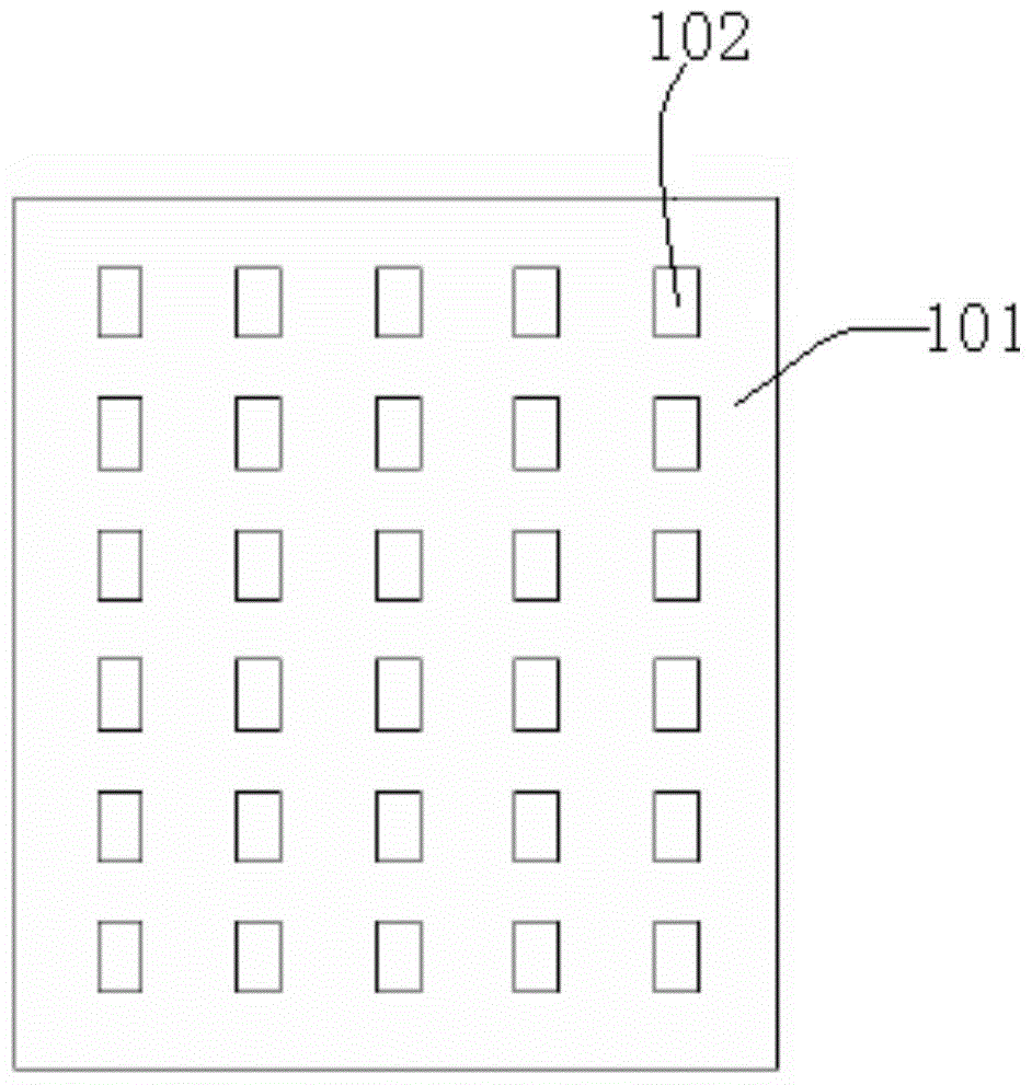
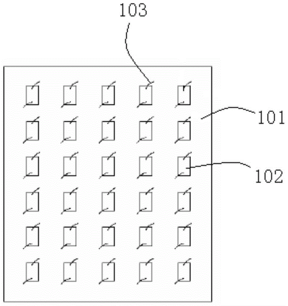
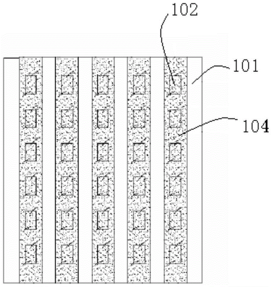
[0032] see figure 2 and Figure 3A —3E, figure 2 It is the manufacturing process flow of the transparent substrate LED light bar of the present invention. It should be noted that the transparent substrate in the present invention includes but is not limited to a glass substrate, an acrylic substrate or a sapphire substrate, and may also be other transparent substrates. The manufacturing process of the transparent substrate LED light bar specifical...


PUM


Abstract

The invention provides a manufacturing process of a transparent substrate LED light bar, which includes the following steps: providing a transparent substrate, one side of the transparent substrate is coated with a transparent conductive layer; solidifying the crystal on the conductive layer of the transparent substrate Install the LED chip; wire bonding, connect the positive and negative poles on the surface of the LED chip with the electrodes on the conductive layer through conductive wires; press the fluorescent glue on both sides of the transparent substrate symmetrically by molding, so that The fluorescent glue covers the LED chips; punching cuts the transparent substrate into several LED light strips. Compared with the prior art, the invention has a simple process, can realize 360° light emission with single-sided crystal bonding, and has better light emission effect.

Description

technical field [0001] The invention relates to the lighting field, in particular to a manufacturing process of a transparent substrate LED light bar. Background technique [0002] With the rapid development of the LED (Light-Emitting Diode, light-emitting diode) industry, many LED manufacturing companies have emerged in the world. The manufacturing process of the existing LED light bar needs to go through two processes, one is LED packaging, and the other is SMT (surface mount technology, SMT for short) patch. The existing LED light strips have many and complicated manufacturing processes, and most of the substrates in the prior art are metal substrates, which are opaque; and most of the LED light strips emit light from one side; each LED chip on the light strip is After encapsulation, it is cut into an independent luminescent particle. [0003] see Figure 1A — 1E, which is a schematic diagram of the manufacturing process structure of the LED light bar in the prior art. ...

Claims


Application Information

Patent Timeline
Patent Type & Authority Patents(China)
IPC IPC(8): H01L25/075H01L33/48H01L33/50
CPCH01L2224/48091H01L2224/48137H01L2924/00014
Inventor 黄勇鑫充国林袁永刚
Owner YANCHENG DONGSHAN PRECISION MANUFACTURING CO LTD
Why Eureka
Try Eureka