Manufacturing process of multi-point touch single-layer film touch sensor

A touch sensor and multi-touch technology, applied in the input/output process of instruments, data processing, calculation, etc., can solve the problems of increased production cost, many unfavorable factors in the process, and high material cost, and achieve a sharp reduction in the cost of production actions , fewer adverse factors in the process, and the effect of reducing production costs

Inactive Publication Date: 2014-07-09
FUJIAN BAOFA PHOTOELECTRIC TECH
View PDF6 Cites 6 Cited by
  • Summary
  • Abstract
  • Description
  • Claims
  • Application Information

AI Technical Summary

Problems solved by technology

[0002] Traditional touch screens are made by silk screen, acid etching or yellow light process. The process is complicated, the factory configuration space is large, the equipment requirements are large, the staffing is large, and the production and operation costs of the workshop are high.
The traditional touch screen production process has low raw material utilization and high material cost; moreover, the production process line is long and the production cycle is long, so it is impossible to achieve rapid proofing
[0003] The production process line is long, it is easy to cause many bad factors in the process, and the product yield is relatively low; the production process requires special chemical solution treatment, which is likely to cause pollution to the workshop and further increase production costs
[0004] The impedance of the electrode pattern produced by the traditional touch screen production process can only be single, and the function of the finished product can only be optimized by software, and the yield rate of the complex electrode pattern cannot be guaranteed. Furthermore, it is difficult to achieve a single-layer thin structure with Multi-touch capacitive screen

Method used


Image

  • Manufacturing process of multi-point touch single-layer film touch sensor
  • Manufacturing process of multi-point touch single-layer film touch sensor
  • Manufacturing process of multi-point touch single-layer film touch sensor

Examples


Embodiment Construction

[0036] The present invention will be further described in detail below in conjunction with the accompanying drawings and embodiments.

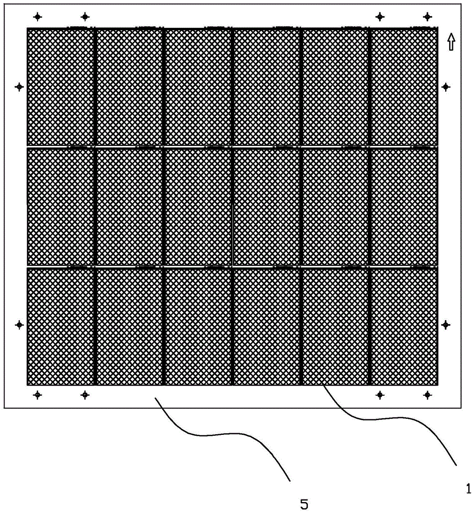
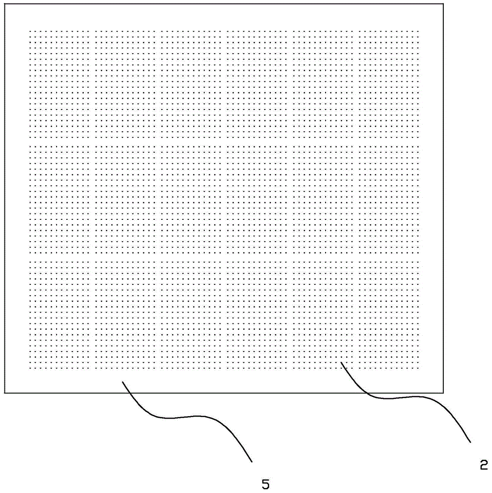
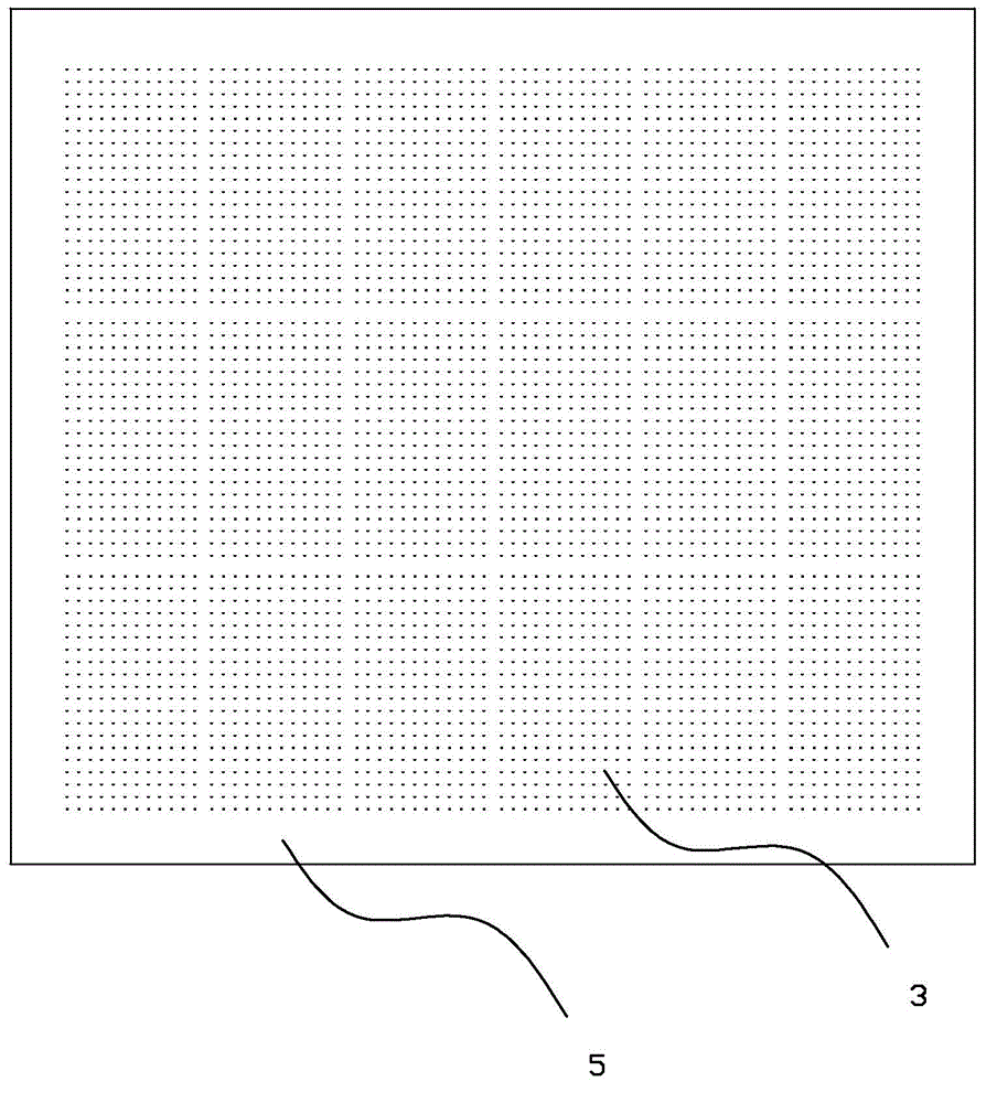
[0037] The invention provides a multi-touch single-layer thin-film touch sensor manufacturing process. Based on the 3D printing process, the functional image of the sensor is printed layer by layer, starting from the bottom layer and superimposed layer by layer; after the functional image is formed, use the traditional The post-forming process of the thin film sensor is the production process of the multi-touch single-layer thin film touch sensor by laminating the functional image with the optical glue, defoaming, cutting and forming.

[0038] details as follows:

[0039] Step 1. Convert the designed electrode pattern and electrode lead 1 pattern, that is, the 2D computer-aided design file, into a 3D three-dimensional computer-aided design data file and input it into the 3D printer, and put the special transparent conductive material (graphene...


PUM


Abstract

The invention relates to a manufacturing process of a multi-point touch single-layer film touch sensor. The process is based on a three-dimensional (3D) printing process to perform layering printing on functional images of the sensor by starting from the bottom layer and overlaying the images layer by layer; after the functional images are formed, the functional images are glued to optical adhesive to be subjected to de-foaming, cutting and forming, and the manufacturing process of the multi-point touch single-layer film touch sensor can be achieved. The manufacturing process of the multi-point touch single-layer film touch sensor has the advantages that the process is single, configuration space of a factory is small, a single 3D printer device is merely required, personnel allocation is small, and producing costs are sharply reduced; the utilization ratio of raw materials is high, and consumables are used for solid printing of functional zone patterns by nearly 100%; proofing can be rapidly achieved, and the production cycle is shortened; the production line is quite short, deficient manufacturing procedure factors are few, and the product yield of the manufacturing process is higher than that of traditional processes; chemical solution treatment is absent, and producing costs are further lowered compared with those of the traditional processes; different dots per inch (dpi), each layer film thickness and the number of layers are set on a 3D printer to manufacture electrode patterns with different impedances.

Description

technical field [0001] The invention relates to a production process of a touch screen, more specifically, to a production process of a multi-touch single-layer thin-film touch sensor. Background technique [0002] Traditional touch screens are all produced by silk screen, acid etching or yellow light process. The process is complicated, the factory configuration space is large, the equipment requirements are large, the staffing is large, and the production and operation costs of the workshop are high. The traditional touch screen production process has low raw material utilization and high material cost; moreover, the production process has a long assembly line and a long production cycle, making rapid proofing impossible. [0003] The long production process line will easily lead to many bad factors in the process and relatively low product yield; the production process requires special chemical solution treatment, which is likely to cause pollution to the workshop and fur...

Claims


Application Information

Patent Timeline
Patent Type & Authority Applications(China)
IPC IPC(8): G06F3/044
Inventor 陈聪卢镇州
Owner FUJIAN BAOFA PHOTOELECTRIC TECH
Why Eureka
Try Eureka