Method for manufacturing transistor

A manufacturing method and transistor technology, which can be used in semiconductor/solid-state device manufacturing, semiconductor devices, electrical components, etc., and can solve problems such as uneven threshold voltage

Active Publication Date: 2014-07-09
SEMICON MFG INT (SHANGHAI) CORP
View PDF5 Cites 5 Cited by
  • Summary
  • Abstract
  • Description
  • Claims
  • Application Information

AI Technical Summary

Problems solved by technology

[0010] The technical problem to be solved by the present invention is that the threshold voltage of the high-k metal gate transistor formed in the prior art is not uniform

Method used


Image

  • Method for manufacturing transistor
  • Method for manufacturing transistor
  • Method for manufacturing transistor

Examples


Embodiment Construction

[0041] The manufacturing method of the metal gate transistor mentioned in the background art is likely to cause irregular damage to the protective layer, and an oxide layer with uneven depth is formed on the surface of the protective layer, resulting in uneven threshold voltage of the transistor.

[0042] In order to solve the above-mentioned technical problems, the inventor made a lot of analysis on the manufacturing method of the above-mentioned metal gate transistor. Through in-depth analysis, the inventor found that:

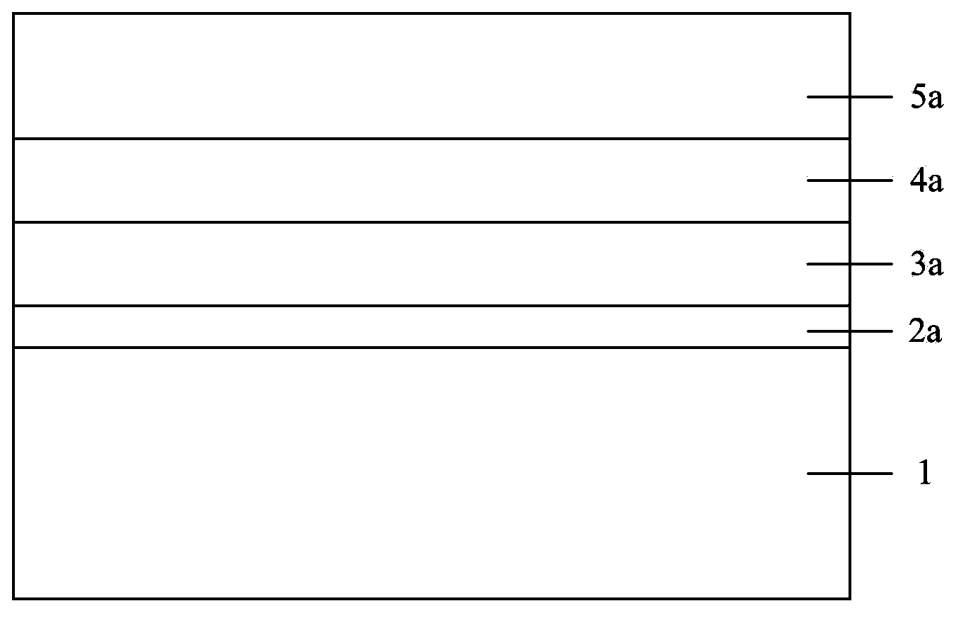
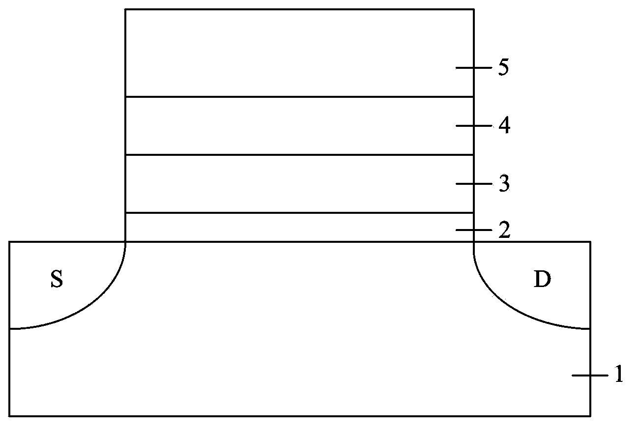
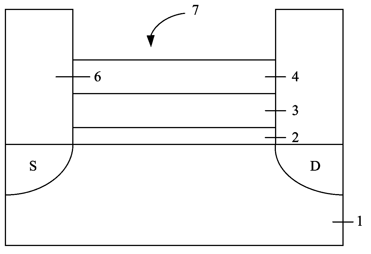
[0043] combined reference figure 2 and image 3, when removing the polysilicon layer 5, dry etching is often used. Due to the high etching rate of the polysilicon layer 5 and the etching effect on the protective layer 4, the polysilicon layer 5 is removed to form a dummy gate. During the process of trench 7, it is easy to cause irregular damage to protective layer 4 by over-etching, and the irregular damage itself will cause uneven threshold voltage. In a...


PUM


Abstract

The invention provides a method for manufacturing a transistor. The method comprises the steps of providing a substrate, wherein a false gate structure is formed on the substrate, the false gate structure comprises a gate dielectric layer, a protective layer located on the gate dielectric layer, an oxide layer located on the protective layer and a false gate located on the oxide layer, the gate dielectric layer is made of oxygen containing materials, and oxygen diffuses to the upper surface of the protective layer, so that an oxidation layer is formed; forming the source electrode and the drain electrode of the transistor after the false gate structure is formed; forming an interlayer dielectric layer on the substrate after the source electrode and the drain electrode are formed, wherein the upper surface of the false gate structure is exposed through the interlayer dielectric layer; eliminating the false gate, wherein a false gate trench is formed in the interlayer dielectric layer; eliminating the oxide layer and the oxidation layer after the false gate trench is formed; forming a gate electrode in the false gate trench after the oxide layer and the oxidation layer are eliminated. By the adoption of the method for manufacturing the transistor, the transistor can obtain an even threshold voltage, and therefore the performance of the transistor is improved.

Description

technical field [0001] The invention belongs to the field of semiconductor manufacturing, in particular to a method for manufacturing a transistor. Background technique [0002] With the continuous reduction of complementary metal oxide semiconductor (CMOS) size, the traditional SiO2 as gate dielectric can no longer meet the needs of the rapid development of integrated circuits. When the thickness of the SiO2 gate dielectric is below 10nm, problems such as tunneling current, vacuum defects, poor reliability, and performance failure will occur, and the leakage current and power consumption will rise sharply. If it cannot be solved well, the power consumption will increase accordingly. Moreover, due to the appearance of the short channel effect, the threshold voltage of the CMOS transistor will be lowered, and the threshold voltage will be unstable. To solve these problems, novel high-k metal gate transistors have been extensively studied and applied. Compared with the tradi...

Claims


Application Information

Patent Timeline
Patent Type & Authority Applications(China)
IPC IPC(8): H01L21/28
CPCH01L21/28247H01L29/401H01L29/6653H01L29/66545
Inventor 王冬江李凤莲王新鹏张海洋
Owner SEMICON MFG INT (SHANGHAI) CORP
Why Eureka
Try Eureka