Oxide thin-film transistor with bottom-gate structure and manufacturing method thereof

A technology of oxide thin films and oxide semiconductors, which is applied in the direction of transistors, semiconductor/solid-state device manufacturing, semiconductor devices, etc., and can solve the problems of TFT device failure and inability to form channel regions, etc.

Active Publication Date: 2014-07-09
SHANGHAI TIANMA MICRO ELECTRONICS CO LTD +1
View PDF8 Cites 18 Cited by
  • Summary
  • Abstract
  • Description
  • Claims
  • Application Information

AI Technical Summary

Problems solved by technology

[0004] Embodiments of the present invention provide a bottom-gate structure oxide thin film transistor and a manufacturing method thereof, which are used to solve the problem that hydrogen ions in the hydrogen-containing passivation layer enter the entire oxide semiconductor layer and cannot form a trench in the prior art. Problems of channel area and TFT device failure

Method used


Image

  • Oxide thin-film transistor with bottom-gate structure and manufacturing method thereof
  • Oxide thin-film transistor with bottom-gate structure and manufacturing method thereof
  • Oxide thin-film transistor with bottom-gate structure and manufacturing method thereof

Examples


Embodiment 1

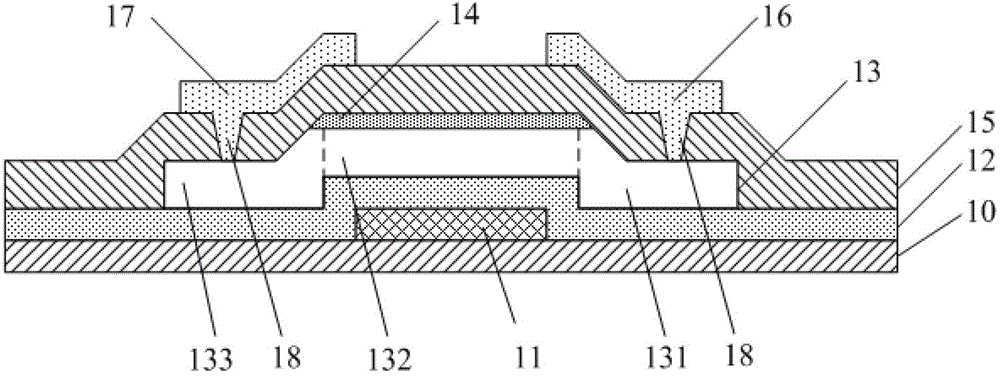
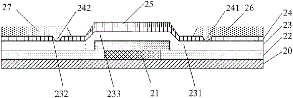
[0046] An embodiment of the present invention provides an oxide TFT with a bottom-gate and bottom-contact structure. The structure of the TFT is as follows: figure 2As shown, it includes: a substrate 20; a gate 21 formed on the substrate 20; a gate insulating layer 22 formed on the gate 21 and the substrate 20 and covering the gate 21; an active layer 23 formed of an oxide The semiconductor is formed on the gate insulating layer 22, including a source region 231, a drain region 232, and a channel region 233 corresponding to the gate 21. The source region 231 and the drain region 232 are doped with hydrogen ions; the hydrogen permeable layer 24 is formed on the On the source layer 23, it is used to control the amount of doped hydrogen ions in the source region 231 and the drain region 232; the etch barrier layer 25 is formed on the hydrogen permeable layer 24 at a position corresponding to the gate 21, and is used to prevent hydrogen ions from entering The channel region 233; ...

Embodiment 2

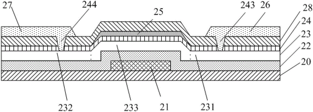
[0088] An embodiment of the present invention provides an oxide TFT with a bottom-gate top-contact structure. The structure of the TFT is as follows: Figure 15As shown, it includes: a substrate 20; a gate 21 formed on the substrate 20; a gate insulating layer 22 formed on the gate 21 and the substrate 20 and covering the gate 21; an active layer 23 formed of an oxide The semiconductor is formed on the gate insulating layer 22, including a source region 231, a drain region 232, and a channel region 233 corresponding to the gate 21. The source region 231 and the drain region 232 are doped with hydrogen ions; the hydrogen permeable layer 24 is formed on the On the source layer 23, it is used to control the amount of doped hydrogen ions in the source region 231 and the drain region 232; the etch barrier layer 25 is formed on the hydrogen permeable layer 24 at a position corresponding to the gate 21, and is used to prevent hydrogen ions from entering Channel region 233; source 26 ...


PUM


Abstract

The invention discloses an oxide thin-film transistor with a bottom-gate structure and a manufacturing method of the oxide thin-film transistor. According to the manufacturing method, the oxide thin-film transistor comprises a substrate, a gate electrode, a gate insulating layer, an active layer, a hydrogen permeation layer, an etching barrier layer, a source electrode and a drain electrode; the gate electrode is formed on the substrate; the gate insulating layer is formed on the gate electrode and the substrate, and the gate electrode is covered with the gate insulating layer; the active layer is formed by an oxide semiconductor on the gate insulating layer, the active layer comprises a source region, a drain region and a channel region corresponding to the gate electrode, and the source region and the drain region are doped with hydrogen ions; the hydrogen permeation layer is formed on the active layer and used for controlling the number of the hydrogen ions doped with the source region and the drain region; the etching barrier layer is formed at the position, corresponding to the gate electrode, of the hydrogen permeation layer, and is used for preventing the hydrogen ions from entering the channel region; the source electrode and the drain electrode are electrically connected to the active layer. According to the scheme of the oxide thin-film transistor with the bottom-gate structure and the manufacturing method of the oxide thin-film transistor, the hydrogen permeation layer is arranged, as a result, it is guaranteed that the channel region can be formed, and then it is guaranteed that a TFT device is effective.

Description

technical field [0001] The invention relates to the field of semiconductor devices, in particular to an oxide thin film transistor with a bottom gate structure and a manufacturing method thereof. Background technique [0002] Thin Film Transistor (TFT) is a basic logic unit device, which has good application prospects in the fields of flat panel display, sensor, memory card, radio frequency identification tag, etc. Therefore, the research and development of TFT is widely received internationally. focus on. [0003] The structure of the existing TFT is as figure 1 as shown, figure 1 The TFT shown in FIG. On the gate insulating layer 12 is the active layer 13, the material of the active layer can be an oxide semiconductor, and the etching stopper layer 14 formed on the active layer 13 is formed on the gate insulating layer 12, the active layer 13 and the etch barrier layer 14 is a hydrogen-containing passivation layer 15, the hydrogen ions in the hydrogen-containing passiv...

Claims


Application Information

Patent Timeline
Patent Type & Authority Applications(China)
IPC IPC(8): H01L29/786H01L29/06H01L21/336
CPCH01L29/66969H01L29/7869
Inventor 翟应腾吴勇
Owner SHANGHAI TIANMA MICRO ELECTRONICS CO LTD
Why Eureka
Try Eureka