Two-dimensional stratified material based SOI (Semicon-on-insulator) base micro loop filter

A two-dimensional layered and filter technology, applied in the direction of instruments, light guides, optics, etc., can solve the problem that the noise of the microring filter cannot be handled well, and achieve the effects of guaranteed performance, good compatibility, and increased extinction ratio

Inactive Publication Date: 2014-07-23
SUZHOU UNIV
View PDF3 Cites 31 Cited by
  • Summary
  • Abstract
  • Description
  • Claims
  • Application Information

AI Technical Summary

Problems solved by technology

The traditional SOI-based microring filter only improves the performance of the filter by changing the size of the microring or changing the waveguide structure, but there is no way to change some essential problems, such as the noise in the microring filter cannot be handled well, In order to improve the 3dB bandwidth, it is necessary to change the structure of the filter, which is a big challenge for the process

Method used


Image

  • Two-dimensional stratified material based SOI (Semicon-on-insulator) base micro loop filter
  • Two-dimensional stratified material based SOI (Semicon-on-insulator) base micro loop filter
  • Two-dimensional stratified material based SOI (Semicon-on-insulator) base micro loop filter

Examples


Embodiment Construction

[0027] The present invention will be described in detail below with reference to the accompanying drawings and in combination with embodiments.

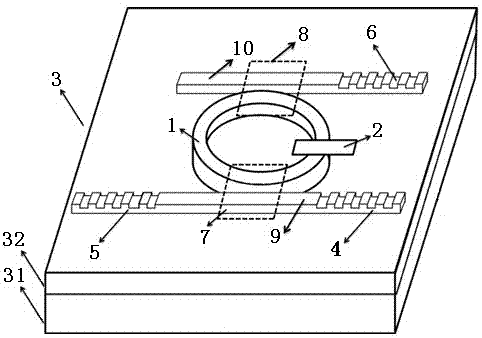
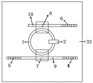
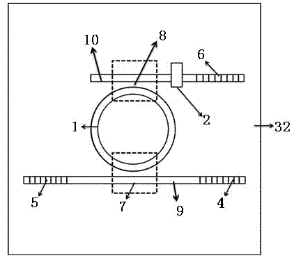
[0028] The present invention is a signal filter device based on a silicon-based two-dimensional layered material designed based on the SOI substrate material. For different thicknesses of the buried oxide layer and the thickness of the top layer of silicon, the corresponding optimal design is also different in order to achieve functional requirements. Therefore, for the convenience of In the description, the substrate material of the present invention defaults to specific implementation parameters, that is, the thickness of the buried oxide layer is 2 μm, and the thickness of the top silicon layer is 340 nm.

[0029] see figure 1 As shown, the SOI-based microring filter based on two-dimensional layered materials includes an SOI substrate 3 composed of a buried oxide layer 31 and a top layer of silicon 32, and a group of SOI microring...


PUM


Abstract

The invention discloses a two-dimensional stratified material based SOI (Semicon-on-insulator) base micro loop filter. The two-dimensional stratified material based SOI base micro loop filter comprises an SOI substrate which is formed by a buried oxide layer and top silicon; an SOI micro loop resonant cavity, input straight waveguide and output straight waveguide are arranged on the top silicon and the input straight waveguide and output straight waveguide are arranged on the upper side and the lower side of the SOI micro loop resonant cavity, so that the SOI waveguide structure is formed; two-dimensional stratified materials cover the SOI waveguide structure; two ends of the input straight waveguide are provided with input end optical grating and direct connection optical grating; one end of the output straight waveguide is provided with output end optical grating; areas of the SOI micro loop resonant cavity, which are close to the input straight waveguide and the output straight waveguide, form into a first coupling area and a second coupling area. Compared with the traditional technology, the two-dimensional stratified material based SOI base micro loop filter has the advantages of being narrow in 3dB band width, high in extinction ratio, less in noise, compatible with CMOS technology and widely applied to the on-chip optical interconnection network in the future due to the fact that the SOI base filter is further filtered due to the saturated absorption effect of two-dimensional stratified materials.

Description

technical field [0001] The invention relates to silicon-based optoelectronics and chip-level optical interconnection technology, in particular to a silicon-on-insulator (SOI)-based signal filter device based on the saturable absorption effect of a two-dimensional layered material. [0002] Background technique [0003] In the past half century, with the development of integrated circuits, the device technology of silicon-based materials has been very mature, and with the continuous reduction of process size, the integration of integrated circuits has been developing rapidly according to Moore's law. The higher integration of chips brings not only an increase in the number of transistors, but also an increase in chip functions and processing speed. However, as feature sizes shrink and integration levels continue to increase, the limitations of microelectronics processes are becoming increasingly apparent. On the one hand, due to the continuous reduction of device line width...

Claims


Application Information

Patent Timeline
Patent Type & Authority Applications(China)
IPC IPC(8): G02B6/293
Inventor 鲍桥梁李鹏飞李绍娟甘胜孙甜
Owner SUZHOU UNIV
Why Eureka
Try Eureka