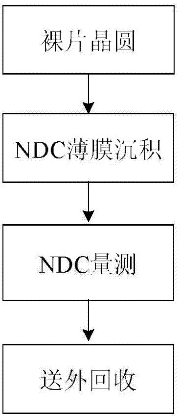
Off-line monitoring method for NDC thin films
A thin-film, off-line technology, used in electrical components, circuits, semiconductor/solid-state device testing/measurement, etc., can solve the problem of high recycling costs, and achieve the effect of reducing recycling times and consumption
- Summary
- Abstract
- Description
- Claims
- Application Information
AI Technical Summary
Problems solved by technology
Method used
Image

Examples
Embodiment 1
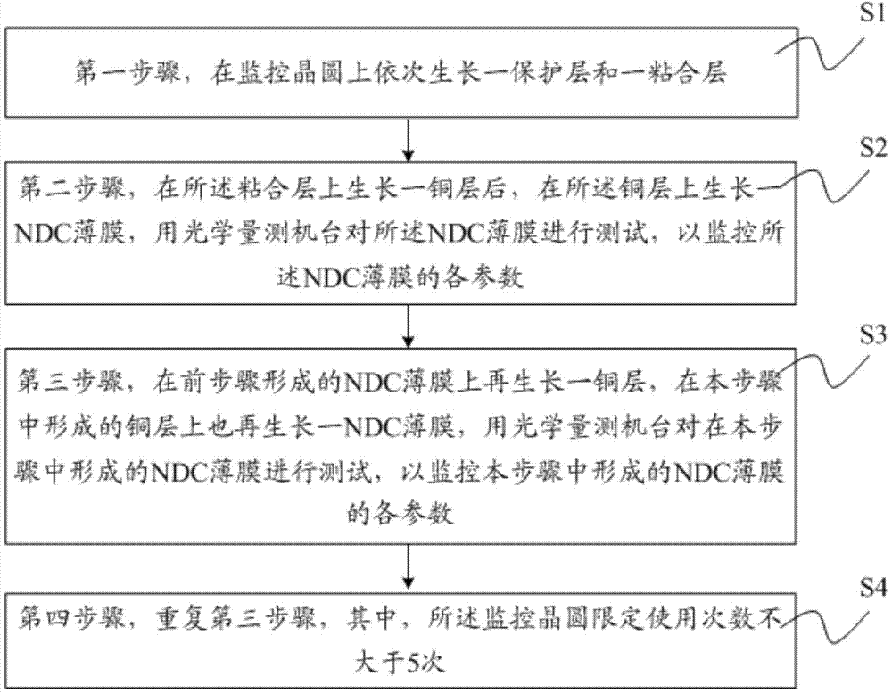
[0028] Specifically, image 3 A flow chart of the off-line monitoring method for NDC films according to Embodiment 1 of the present invention is schematically shown.
[0029] like image 3 shown, combined with Figure 5 , the off-line monitoring method for NDC film according to Embodiment 1 of the present invention comprises:
[0030] In the first step S1 , a protective layer 200 and an adhesive layer 300 are sequentially grown on the monitor wafer 100 from bottom to top.
[0031] Wherein, the protective layer 200 is formed by the silicon oxide thin film material by PECVD method, and the formed thickness is If the protective layer is too thin, the silicon chip cannot be protected; if the protective layer is too thick, it will easily cause waste of materials and increase the cost. The silicon chip mentioned here is the monitor wafer 100 . The material used for the adhesive layer 300 is tantalum nitride / tantalum (TaN / Ta), and the thickness of the adhesive layer 300 formed ...
Embodiment 2
[0038] Specifically, Figure 4 Based on the first embodiment of the present invention, it further schematically shows the flow chart of the off-line monitoring method for NDC film according to the second embodiment of the present invention.
[0039] like Figure 4 shown, combined with Figure 5 , according to the second embodiment of the present invention, the off-line monitoring method for NDC film includes:
[0040] In the first step S1 , a protective layer 200 and an adhesive layer 300 are sequentially grown on the monitor wafer 100 from bottom to top.
[0041] Wherein, the protective layer 200 is formed by silicon nitride film material by PECVD method, and the formed thickness is If the protective layer is too thin, the silicon chip cannot be protected; if the protective layer is too thick, it will easily cause waste of materials and increase the cost. The silicon chip mentioned here is the monitor wafer 100 . The material used for the adhesive layer 300 is tantalum n...
PUM
 Abstract
Description
Claims
Application Information
 - R&D
- Intellectual Property
- Life Sciences
- Materials
- Tech Scout
- Unparalleled Data Quality
- Higher Quality Content
- 60% Fewer Hallucinations
Browse by: Latest US Patents, China's latest patents, Technical Efficacy Thesaurus, Application Domain, Technology Topic, Popular Technical Reports.
© 2025 PatSnap. All rights reserved.Legal|Privacy policy|Modern Slavery Act Transparency Statement|Sitemap|About US| Contact US: help@patsnap.com